Curable resin composition for nanoimprint

a technology of nano-imprinting and resin composition, which is applied in the direction of photomechanical equipment, manufacturing tools, instruments, etc., can solve the problems of line edge roughness to come to the surface, modern steppers are a considerable cost factor in microchip production, and cost explosion, so as to improve patterning accuracy, improve mold releasability, and improve mold releasability

Inactive Publication Date: 2013-09-10
DAICEL CHEM IND LTD
View PDF21 Cites 9 Cited by
  • Summary
  • Abstract
  • Description
  • Claims
  • Application Information

AI Technical Summary

Benefits of technology

[0013]Accordingly, an object of the present invention is to provide a photocurable resin composition for nanoimprint and a cured article therefrom, which photocurable resin composition is suitable for nanoimprinting and gives a cured article having satisfactory adhesion to a substrate and being satisfactorily releasable from a mold. The nanoimprinting enables more economical fine structuring (microstructuring) of electronic components with substantially lower line edge roughness than photolithography which gives both a high resolution and a satisfactory aspect ratio.
[0015]After intensive investigations, the present inventors have found that accuracy in transfer can be improved by adding a specific compound to a resin composition for nanoimprint used as a transfer resist (nanoimprint resist), which specific compound helps the transfer resist to have remarkably improved mold releasability without significantly lowering adhesion to the substrate.
[0026]The present invention adopts a cationic curing system and / or free-radical curing system to a resist for producing fine structures (e.g., semiconductor materials, flat screens, holograms, structures for media, micromechanical components, and sensors) in the field of microlithography and thereby dramatically improves mold releasability (releasability from the mold). Poor mold releasability remarkably impedes improvements of patterning accuracy. The present invention can thereby give fine structures with excellent pattern shapes but with less defects and, in particular, can stably perform patterning with a small thickness of residual film. The present invention provides curable resin compositions for nanoimprint and cured articles therefrom, which show excellent adhesion to the substrate and are satisfactorily releasable from the mold.Best Modes for Carrying Out the Invention
[0028]In the compound A, the hydrophobic functional group is effective for lowering adhesion to a mold when the coated film is removed from an adherend plate such as glass plate as the mold and is thereby effective for improving releasability from the adherend plate (mold). The reactive functional group is necessary for built-in of the compound A into the cured article derived from the curable monomer component and helps the cured article to have higher adhesion to the substrate such as glass plate.
[0030]For improving the mold releasability while maintaining satisfactory adhesion to the substrate, the compound to be added having a reactive functional group and a hydrophobic functional group in the same molecular skeleton should be segregated in the coated film and should therefore have poor immiscibility (compatibility) with the curable monomer component. For these purposes, the hydrophobic functional group is very important. Particularly when adopted to lithography use, this technique stably achieves patterning with a small thickness of residual film, which small thickness of residual film is significantly important in such lithography use.
[0065]In an embodiment, the photocurable resin composition according to the present invention further contains, as a component, a compound that is expandable upon setting (setting-expandable compound). The resulting photocurable resin composition gives patterns with further excellent shapes, in which shrinkage on curing is further controlled.

Problems solved by technology

However, the size of such a small structure of about 32 nm or less approximates to the size of a resin used, and this causes problems such as line edge roughness to come to the surface.
On the other hand, the increasingly high requirements with respect to resolution, wall slope, and aspect ratio (ratio of height to resolution) result in a cost explosion in the case of the apparatuses required for photolithographic structuring, such as masks, mask aligners, and steppers.
In particular, owing to their price of several billion yen, modern steppers are a considerable cost factor in microchip production.
However, this technique still has many problems from the viewpoint of productivity.
Owing to common thickness variations of about 100 nm over the total wafer surface, it is not possible to structure 6-, 8-, and 12-inch wafers in one step with a rigid stamp.
Thus, a complicated “step and repeat” method would have to be used, which, however, is unsuitable owing to the reheating of already structured neighboring areas.
The resist materials used exhibit sufficient wetting with respect to the substrate but are not suitable for a lift-off method, nor do they have sufficient etch resistance.
This technique, however, sacrifices adhesion to the substrate for the improvement in mold releasability and is thereby unsuitable for the formation of a satisfactory pattern, owing to the free-radical curing, non-solvent system employed as a reaction system.
However, when adopted to such use, the nanoimprint technique gives a film having insufficient adhesion to the substrate.

Method used


Image

  • Curable resin composition for nanoimprint
  • Curable resin composition for nanoimprint
  • Curable resin composition for nanoimprint

Examples


examples

[0135]The present invention will be illustrated in further detail with reference to several working examples below. It should be noted, however, that these examples are never construed to limit the scope of the present invention.

examples 1 to 11

, Comparative Examples 1 to 3

1) Preparation Method of Coated Films

[0136]A silicon substrate used herein was a 4-inch silicon wafer which had been preliminarily treated with hexamethyldisilazane.

[0137]A series of photocurable resin compositions for nanoimprint was prepared according to a known procedure in a spin coater using a compound (A) having a reactive functional group and a hydrophobic functional group in the same molecular skeleton, a curable monomer component (B), an initiator (C), a sensitizer (D), nanoscale particles (E), a binder resin (film-forming aid; F), and a solvent (G) as given in Table 1. Specific compounds as the respective components in Table 1 are shown below.

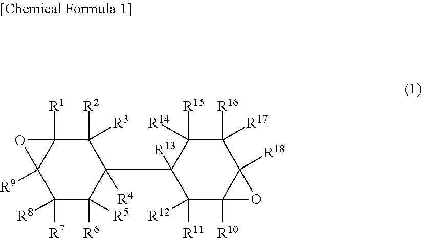
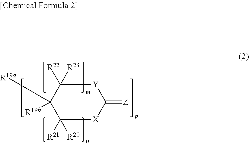
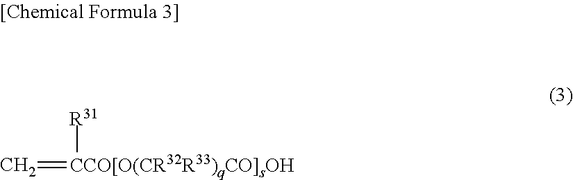
[0138]Compounds having a reactive functional group and a hydrophobic functional group in the same molecular skeleton: shown in Table 2.

[0139]Curable monomer components: shown in Table 3.

[0140]Initiators

[0141]C-1: 4-Methylphenyl[4-(1-methylethyl)phenyliodonium tetrakis(pentafluorophenyl)borate; PI2074 suppl...


PUM

PropertyMeasurementUnit
sizeaaaaaaaaaa
thicknessaaaaaaaaaa
thicknessaaaaaaaaaa

Abstract

Disclosed is a photocurable resin composition for nanoimprint, containing a curable monomer component with or without a binder resin. The composition further contains 0.001 to 5 parts by weight of a compound having a reactive functional group and a hydrophobic functional group in the same molecular skeleton, per 100 parts by weight of the total amount of the curable monomer component and binder resin. Preferably, the reactive functional group is at least one functional group selected from the group consisting of hydroxyl groups, epoxy groups, vinyl ether groups, oxetanyl groups, alkoxysilane groups, and free-radically polymerizable vinyl groups, and the hydrophobic functional group is at least one functional group selected from the group consisting of fluorine-containing groups, alkylsilane groups, alicyclic hydrocarbon groups, and aliphatic hydrocarbon groups having 4 or more carbon atoms.

Description

TECHNICAL FIELD[0001]The present invention relates to a photocurable resin composition for nanoimprint and a cured article obtained therefrom, which photocurable resin composition is suitable for the highly accurate formation of a fine pattern through nanoimprinting in the field of microlithography. The present invention also relates to a process for the production of a fine structure using the photocurable resin composition, and to a fine structure produced by the process.BACKGROUND ART[0002]The miniaturization of electronic components, for which a resolution down to the range of less than 1 μm is required, has been achieved substantially by photolithographic techniques. To give further smaller structures, miniaturization is being achieved by the progress of ArF lithography and ArF immersion lithography technologies. However, the size of such a small structure of about 32 nm or less approximates to the size of a resin used, and this causes problems such as line edge roughness to co...

Claims


Application Information

Patent Timeline
Patent Type & Authority Patents(United States)
IPC IPC(8): C08F2/46C08J3/28
CPCB82Y10/00B82Y40/00C08F2/48G03F7/027G03F7/038G03F7/0002Y10T428/24479G03F7/0048B29C2059/023H01L21/0274
Inventor MIYAKE, HIROTOIYOSHI, SHUSO
Owner DAICEL CHEM IND LTD
Why Eureka
Try Eureka