Microfluidic device and manufacture thereof

a microfluidic device and microfluidic technology, applied in the field of microreactors, can solve the problems of high cost of silicon devices, difficult control of surface states effectively within such structures, and inability to withstand temperatures of more than 200.degree. c. to 300.degree. c. over a prolonged period

Inactive Publication Date: 2003-07-22
CORNING INC
View PDF8 Cites 58 Cited by
  • Summary
  • Abstract
  • Description
  • Claims
  • Application Information

AI Technical Summary

Benefits of technology

The microfluidic device and method of manufacturing such microfluidic devices results in a number of advantages over other microfluidic devices and manufacturing techniques known in the art. For example, the vacuum-forming aspect of the present invention is a technique that is compatible with low-cost production and significant yield. In addition, vacuum-forming enables high aspect ratios without the use of expensive techniques such as physical etching.

Problems solved by technology

For example, devices made of polymers cannot withstand temperatures of more than 200.degree. C. to 300.degree. C. over a prolonged period.
Moreover, it is often difficult to control surface states effectively within such structures.
Silicon devices are expensive, incompatible with certain biological fluids, and the semiconductive nature of silicon gives rise to problems with implementing certain pumping techniques, such as electro-hydrodynamic pumping and electro-osmotic pumping.
Devices made of metal are liable to corrode, and in like manner they are typically not compatible with certain biological fluids.
Those etching technologies give rise to hollows in a glass substrate and they are not entirely satisfactory to implement.
Isotropic chemical etching does not enable significant aspect ratios to be obtained, while physical etching is difficult to implement, in particular because of its high cost and limited production capacity.
That technique is expensive, and difficult to implement insofar as it is highly sensitive to dust and insofar as the surface of each layer that is to come into contact must be as flat as possible in order to provide high quality sealing.
Nevertheless, it is not impossible for the fluid inlet and / or outlet to be provided directly via one of the recesses in the one-piece structure opening out directly to the outside.
Such aspect ratios generally cannot be obtained by isotropic chemical etching.
Eliminating volatile components from a complex three-dimensional structure is always a problem, since the gases must be able to escape without damaging the structure.

Method used


Image

  • Microfluidic device and manufacture thereof
  • Microfluidic device and manufacture thereof
  • Microfluidic device and manufacture thereof

Examples


Embodiment Construction

The invention is illustrated by the following example:

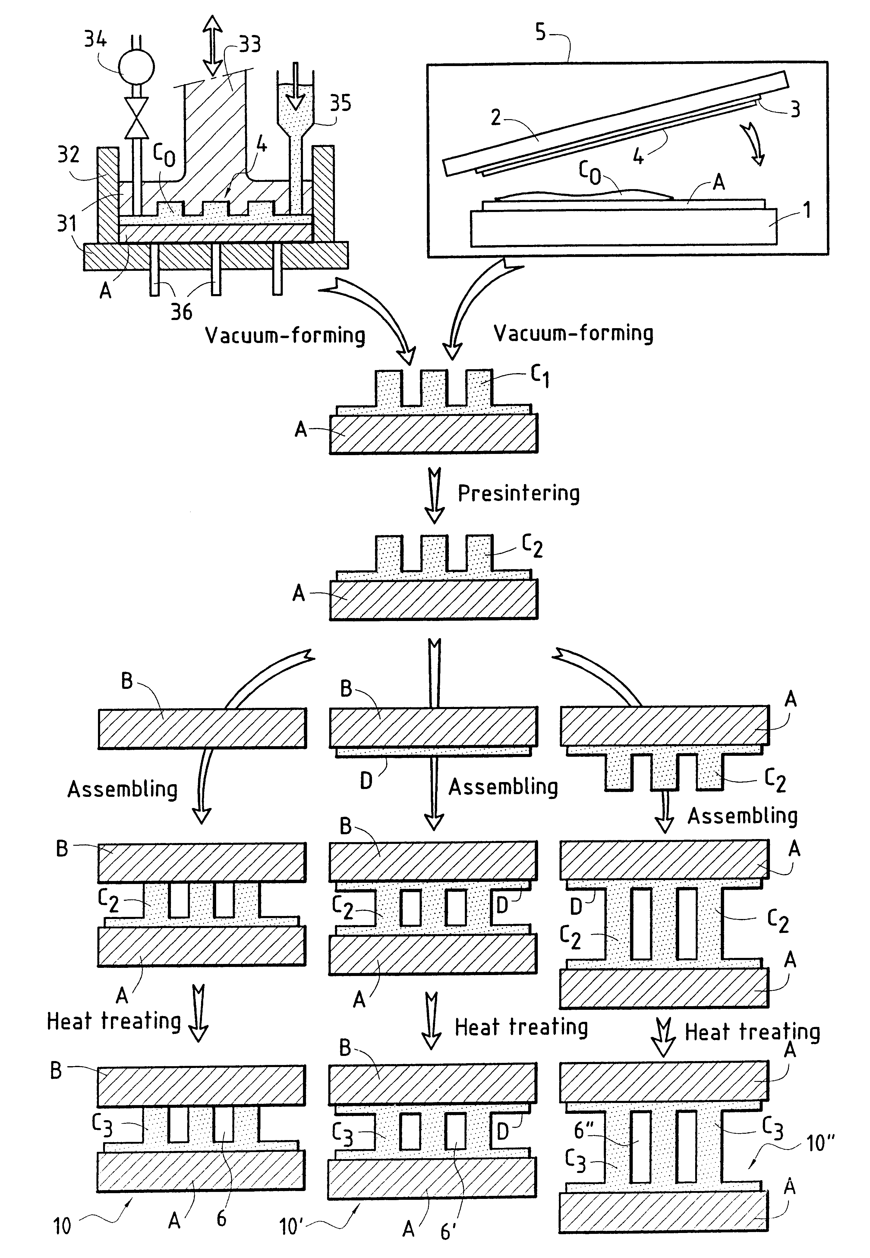
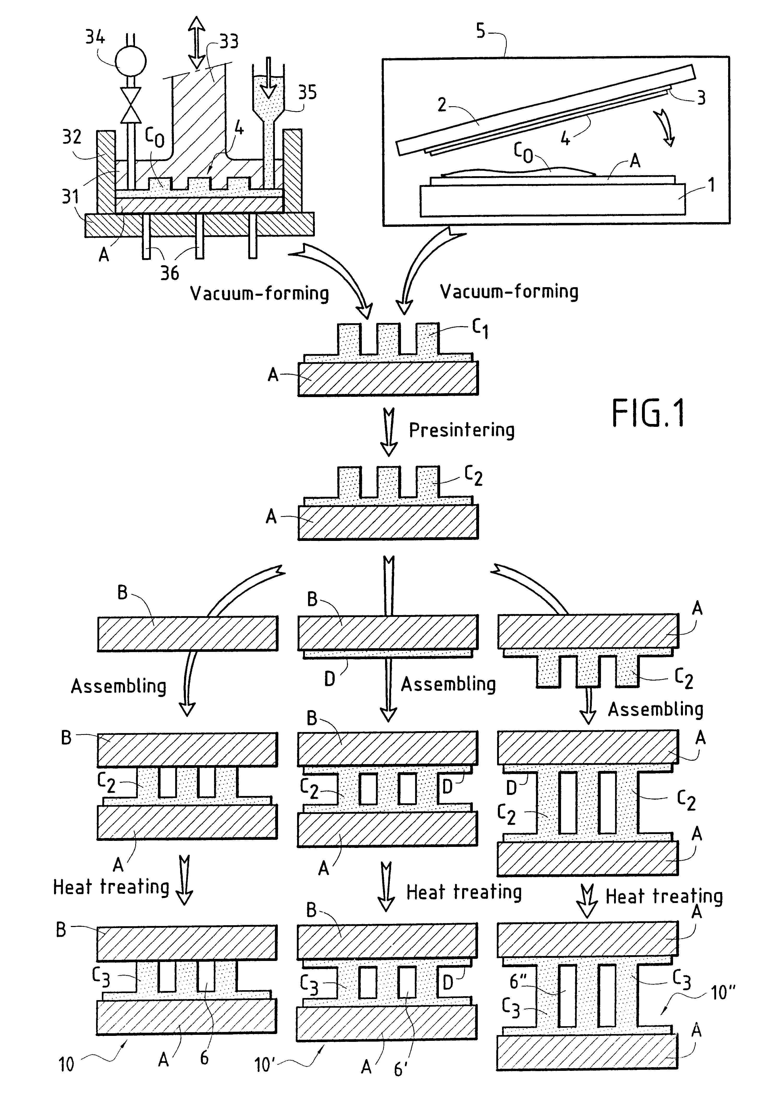
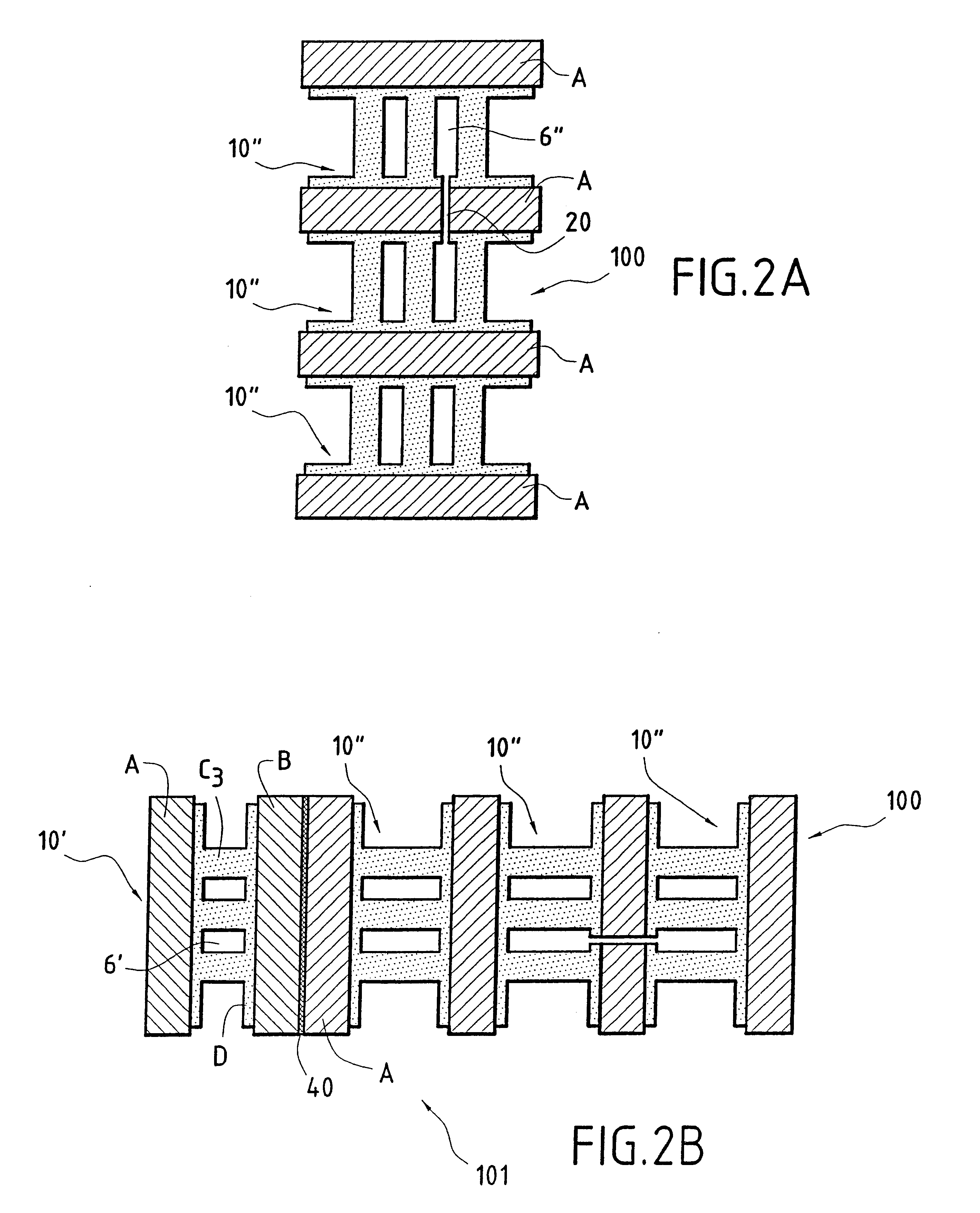
Microreactors of the 10' type (as shown diagrammatically in FIG. 4) were made using a baseplate of alkali-lime type glass on which electrodes were deposited (which electrodes can be used for local heating, for temperature control, or as probes). The thickness of the first substrate should be at least 200 .mu.m, and should generally lie in the range of about 200 .mu.m to about 3 millimeters (mm). Structures in relief were formed on the glass plate by microforming glass, the structures having a width Iying in the range of about 100 .mu.m to about 300 .mu.m and a height of up to approximately 800 .mu.m; the widths of the resulting capillaries (i.e. recesses) lay in the range of about 50 .mu.m to more than about 1000 .mu.m. Passages were drilled in the appropriate locations to put recesses of the device into communication with the outside. Thereafter, a cover plate of alkali-lime glass was put into place on the drilled glass plate (t...


PUM

PropertyMeasurementUnit
temperaturesaaaaaaaaaa
aspect ratiosaaaaaaaaaa

Abstract

The present invention relates to microfluidic devices and to their method of manufacture. The microfluidic devices are original by their specific structure (of sandwich type) and by the materials from which they are made (mainly glasses, glass ceramics, ceramics), and also by their specific method of manufacture, which is based on a vacuum-forming operation. The microfluidic device includes a first assembly including a microstructure and a first substrate, wherein the microstructure is constructed and arranged on the substrate under vacuum. A second assembly includes a second substrate positioned on the microstructure after the first assembly is presintered and adhered thereto by heat treatment to form a one-piece microstructure defining at least one recess between the first and second substrates.

Description

This application claims the benefit of French Patent Application No. 01 12500, filed on Sep. 28, 2001, in the names of Guillermo Guzman and Jean-Pierre Themont, the entire content of which is incorporated herein by reference.1. Field of the InventionThe present invention relates generally to:the field of microreactors and more particularly to a microfluidic device and a method of manufacturing such microfluidic devices.2. Technical BackgroundMicrofluidic devices are structures familiar to those skilled in the art, structures for which numerous applications have already been described, in particular in references such as: Microreaction Technology, 3.sup.rd International Conference on Microreaction Technology; edited by W. Ehrfeld, published by Springer-Verlag, Berlin (2000); and Micro-total Analysis Systems 2000, edited by A. Van Den Berg, W. Olthius, and P. Bergveld, published by Kluwer Ac Publishers (2000). Within such structures, in volumes that are small (having a characteristic ...

Claims


Application Information

Patent Timeline
Patent Type & Authority Patents(United States)
IPC IPC(8): B81C1/00B81B1/00B01J19/00B01L3/00B81C99/00C03B19/06C03B23/20
CPCB81C1/00071B81C1/00119C03B19/063C03B23/20B01L3/5027B81B2201/058B81B2203/0353B81C2201/019B81C2201/036Y10T137/0391Y10T137/0402Y10T137/6416Y10T137/2224B33Y80/00
Inventor GUZMAN, GUILLAUMETHEMONT, JEAN-PIERRE
Owner CORNING INC
Why Eureka
Try Eureka