Method for producing electroluminescent element

a technology of electroluminescent elements and methods, applied in the field of methods for producing el elements, can solve the problem that the methods cannot provide all the possibilities of el elements

Inactive Publication Date: 2002-06-13
DAI NIPPON PRINTING CO LTD
View PDF0 Cites 55 Cited by
  • Summary
  • Abstract
  • Description
  • Claims
  • Application Information

AI Technical Summary

Benefits of technology

0148] The first embodiment of the EL element of the present invention is an EL element having at least one patterned organic EL layer, and is characterized in that the EL element does not have any of a partition, a structure aiding patterning, and surface treatment aiding patterning.
0149] Though the EL element of the present embodiment has an patterned organic EL layer, it does not have any of a partition, a structure aiding patterning, and surface treatment aiding patterning. Consequently, it has an advantage that it is advantageous in respect of cost.

Problems solved by technology

However, these methods could not provide an EL element being possible to realize all of the high luminous efficiency, the high light takeout efficiency, the simplicity of the production process, and the formation of highly fine patterns.

Method used


Image

  • Method for producing electroluminescent element
  • Method for producing electroluminescent element
  • Method for producing electroluminescent element

Examples


example 1

When a Luminous Layer is Made in a Single Layer

[0190] (Patterning of a Buffer Layer)

[0191] A patterned ITO substrate of 3 inches square and 1.1 mm in thickness was washed and used in this example as a substrate and the first electrode layer.

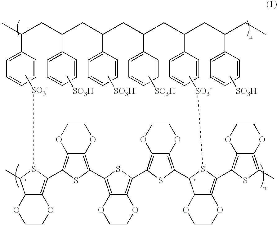
[0192] The spin coating of the substrate was carried out by dropping 0.5 ml of a coating liquid for a buffer layer shown in the following chemical formula (1) (poly-3,4-ethylenedioxythiophene / polystyrenesulphonate (PEDT / PSS): made by Bayer AG (Baytron P)) in the center part of the substrate. 2

[0193] A buffer layer was formed by holding the spin coated substrate at 2500 rpm for 20 seconds, and then the buffer layer was dried at 150.degree. C. for 5minutes. As a result, the film thickness became 800 .ANG..

[0194] The spin coating of the substrate was carried out by dropping 2 ml of positive photoresist liquid (OFPR-800 made by Tokyo Ohka Kogyo Co., Ltd.) in the center part of the substrate. A resist layer was formed by holding the spin coated substr...

example 2

When a Luminous Layer is Made in Three Layers

[0203] A buffer layer was patterned similarly to Example 1.

[0204] The spin coating of the substrate where a buffer layer had been patterned was carried out as the first luminous layer by dropping 2 ml of a 1 wt % xylene solution of luminescent polymer MEH-PPV, which is a polyparaphenylene vinylene derivative, in the center part of the substrate. A luminous layer was formed by holding the spin coated substrate at 2000 rpm for 10 seconds. As a result, the film thickness became 800 .ANG..

[0205] The spin coating of the substrate was carried out by dropping 2 ml of positive photoresist liquid (OFPR-800 made by Tokyo Ohka Kogyo Co., Ltd.) in the center part of the substrate. A resist layer was formed by holding the spin coated substrate at 500 rpm for 10 seconds and then holding at 2000 rpm for 20 seconds. As a result, the film thickness became about 1 .mu.m. The resist layer was prebaked at 80.degree. C. for 30 minutes. After that, the layer w...

example 3

The Change of the Solvent

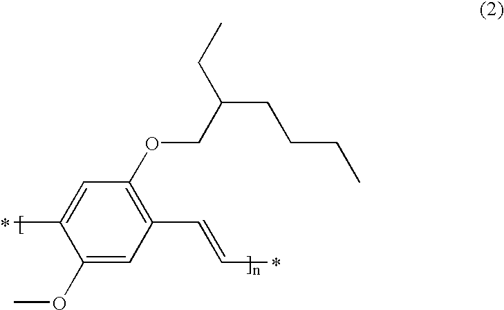
[0214] An EL element was manufactured in the same way as Example 1 except that polyvinylcarbazole shown by the following chemical formula (3) was used as a luminous layer and toluene as a solvent for the luminous layer. 4

[0215] Though the resolution of the obtained pattern depends on the resolving power of the positive resist, the resolution of 10 .mu.m, which is impossible by the conventional methods of the vapor deposition mask method and the inkjet method, and the highly fine lines could be formed in this example.

[0216] (The Evaluation of the Luminous Properties of the EL Element.)

[0217] ITO electrode (the first electrode) side and Ag electrode (the second electrode) side were connected to an anode and a cathode, respectively, and were applied with direct current from a source meter. When 15 V was applied, luminescence was observed, and it was evaluated that there was no deterioration in the voltage of starting luminescence due to patterning with the use ...


PUM

PropertyMeasurementUnit
thicknessaaaaaaaaaa
distanceaaaaaaaaaa
thicknessaaaaaaaaaa

Abstract

The main object of the present invention is to provide a method for producing an EL element for realizing the high luminous efficiency, the high light takeout efficiency, the simplicity of the production process, and the formation of highly fine patterns. In order to achieve the above-mentioned object, the present invention provides a method for producing an EL element wherein at least one organic EL layer constituting the EL element is patterned by the use of a photolithography method.

Description

[0001] The present invention relates to a method for producing an electroluminescent element (may be referred to as an abbreviation of EL) in which a pattern is formed.[0002] EL elements attract attention as spontaneously emitting flat panel display elements in which positive holes and electrons, which have been poured into from opposed electrodes, are combined in a luminous layer to generate energy, and the energy excites fluorescent material in luminous layer to emit light of a color corresponding to the fluorescent material. Among them, an organic thin film EL display using an organic material as a luminescent material has such a high luminous efficiency that high intensity luminescence can be realized even if applied voltage is a little less than 10 V, is possible to emit light with a simple element structure, and is expected to be applied to low-cost simple expression displays such as advertisements and the like in which specific patterns are emitted and displayed.[0003] In the...

Claims


Application Information

Patent Timeline
Patent Type & Authority Applications(United States)
IPC IPC(8): G03F7/00H05B33/10H01L27/32H01L51/00H01L51/30H01L51/40
CPCG03F7/0007H01L27/32H01L51/0018H01L51/0037H01L51/56H01L51/0042H01L51/0059H01L51/0081H01L51/0038H10K59/00H10K71/233H10K85/146H10K85/114H10K85/1135H10K85/631H10K85/324H10K71/00H05B33/10
Inventor KASHIWABARA, MITSUHIRO
Owner DAI NIPPON PRINTING CO LTD
Why Eureka
Try Eureka