Electrical-optical package with capacitor DC shunts and associated methods

a technology of capacitor dc shunt and optical package, which is applied in the direction of optics, optical elements, instruments, etc., can solve the problems of complex and expensive package for a high-power cpu, negatively affecting chip reliability, and high temperatur

Inactive Publication Date: 2003-09-23
INTEL CORP
View PDF3 Cites 24 Cited by
  • Summary
  • Abstract
  • Description
  • Claims
  • Application Information

AI Technical Summary

Problems solved by technology

A large power dissipation in the leads results in higher temperatures, which negatively impacts chip reliability.
Thus, the package for a high-power CPU tends to be complicated and expensive.

Method used


Image

  • Electrical-optical package with capacitor DC shunts and associated methods
  • Electrical-optical package with capacitor DC shunts and associated methods
  • Electrical-optical package with capacitor DC shunts and associated methods

Examples


Embodiment Construction

In the following detailed description of the embodiments of the invention, reference is made to the accompanying drawings that form a part hereof, and in which is shown by way of illustration specific embodiments in which embodiments of the invention may be practiced. These embodiments are described in sufficient detail to enable those skilled in the art to understand and implement them, and it is to be understood that other embodiments may be utilized and that changes may be made without departing from the scope of the present disclosure. The following detailed description is, therefore, not to be taken in a limiting sense, and the scope of embodiments of the present invention is defined only by the appended claims.

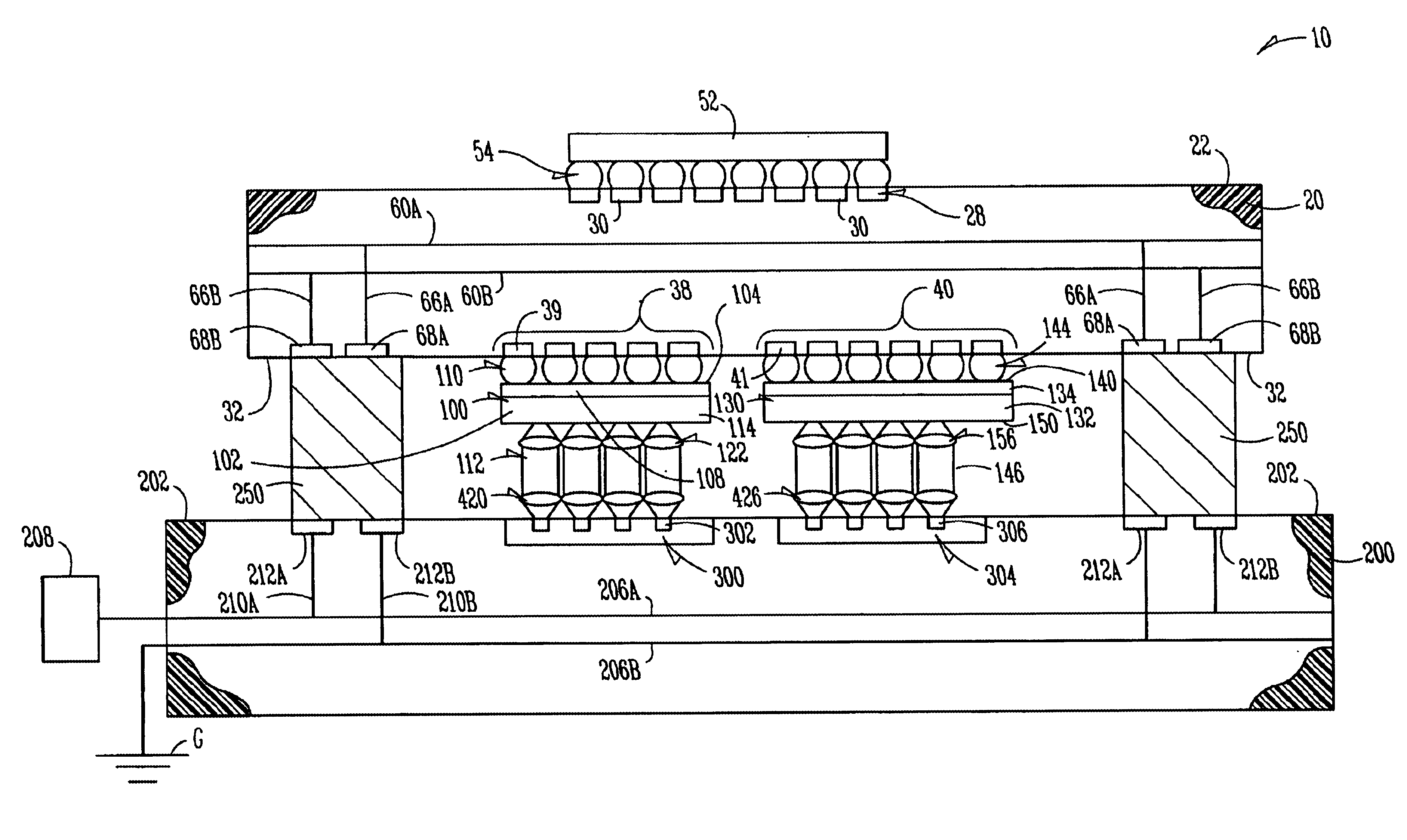
FIG. 1A is a side view of an optical-electrical (OE) package 10 in accordance with one embodiment of the present invention. OE package 10 includes a substrate package (hereinafter, "substrate") 20 having an upper surface 22 with a set 28 of contact-receiving members 30. ...


PUM


Abstract

An optical-electrical (OE) package includes a substrate electrically coupled to a motherboard via one or more capacitor DC shunts (CDCSs). In one embodiment, the substrate includes an IC chip electrically coupled to a first set of contact-receiving members on an upper surface of the substrate. The substrate also includes a light-emitting package and a photodetector package electrically coupled to respective second and third sets of contact-receiving members on the substrate lower surface. The substrate has internal wiring that electrically interconnects the IC chip, the light-emitting package and the photodetector array. The light-emitting package and the photodetector array are optically coupled to respective first and second waveguide arrays formed in or on the motherboard. The CDCSs mitigate noise generated by the IC chip by serving as a local current source.

Description

Embodiments of the present invention relate to integrated circuit packaging and, in particular, relate to integrated circuit packages with optical interconnects.BACKGROUND INFORMATIONThe manufacturing of electronic and optoelectronic integrated circuits (ICs) involves complex lithographic processes to form microscopic solid-state devices and circuits in semiconductor wafers. These lithographic processes typically include forming layers of material on the wafer, patterning the layers, doping the substrate and / or the patterned layers, and heat-treating (e.g., annealing) the resulting structures. These processes are repeated to build up the IC structure. The result is a wafer containing a large number of ICs.A "wafer sort" is then performed, wherein each IC chip on the wafer is electrically tested for functionality. The wafer is then separated ("diced") into the individual IC chips, which are then "packaged" individually or in groups for incorporation onto a printed circuit board (PCB)...

Claims


Application Information

Patent Timeline
Patent Type & Authority Patents(United States)
IPC IPC(8): G02B6/43H01L31/12G02B6/42
CPCG02B6/43H01L31/12G02B6/4232H01L2224/16225
Inventor LI, YUAN-LIANG
Owner INTEL CORP
Why Eureka
Try Eureka