Finishing components and elements

a technology of finishing components and components, applied in the field of finishing components and elements, can solve the problems of reducing the flexibility of adding finishing enhancers, limiting the versatility of some demanding finishing applications, and affecting the quality of finished components, so as to improve the finishing method reduce manufacturing costs, and improve the effect of finishing the cost of semiconductor wafer surfaces

Inactive Publication Date: 2003-11-04
SEMCON TECH
View PDF71 Cites 46 Cited by
  • Summary
  • Abstract
  • Description
  • Claims
  • Application Information

AI Technical Summary

Benefits of technology

It is an advantage of this invention to improve the finishing method for semiconductor wafer surfaces to make them as perfect as possible. It is an advantage of this invention to make finishing elements with a lower cost of manufacture and thus also reduce the cost of finishing a semiconductor wafer surface. It is an advantage of this invention develop a heterogeneous finishing element surface having local regions which improve versatility of the finishing elements and the methods of finishing semiconductor wafers which result. It is also an advantage of the invention to develop finishing element having local regions reinforced with a continuous phase material. It is further an advantage of the...

Problems solved by technology

Current finishing elements can suffer from being costly to manufacture.
Also current finishing elements for semiconductor wafers have relatively homogenous surfaces which inherently limits their versatility in some demanding finishing applications.
Still further, lack of a continuous phase matrix on their surface can reduce the flexibility to add finishing enhancers.
Still further, a lack of the above characteristics in a finishing element reduces the versatility of ...

Method used


Image

  • Finishing components and elements
  • Finishing components and elements
  • Finishing components and elements

Examples


Embodiment Construction

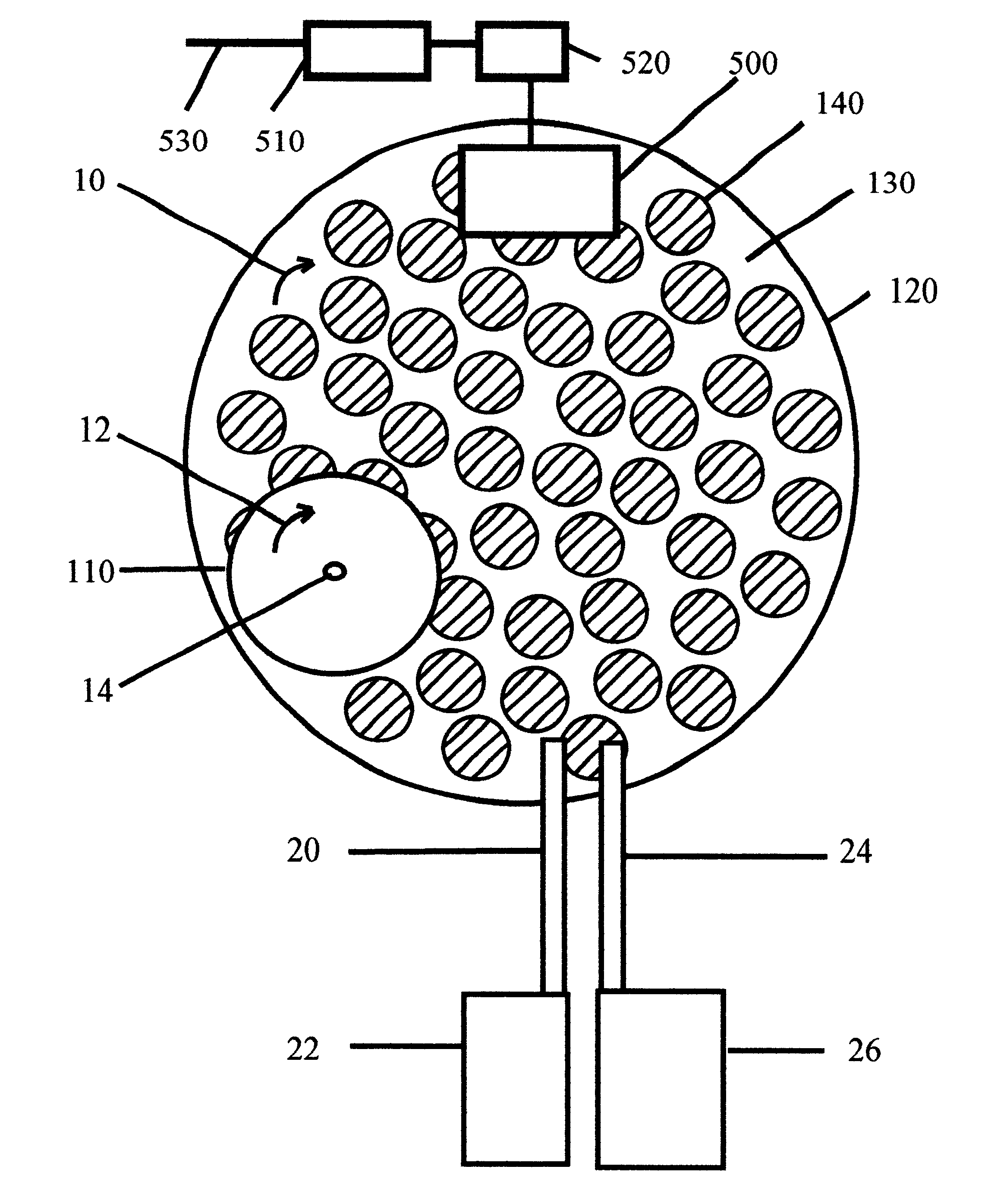
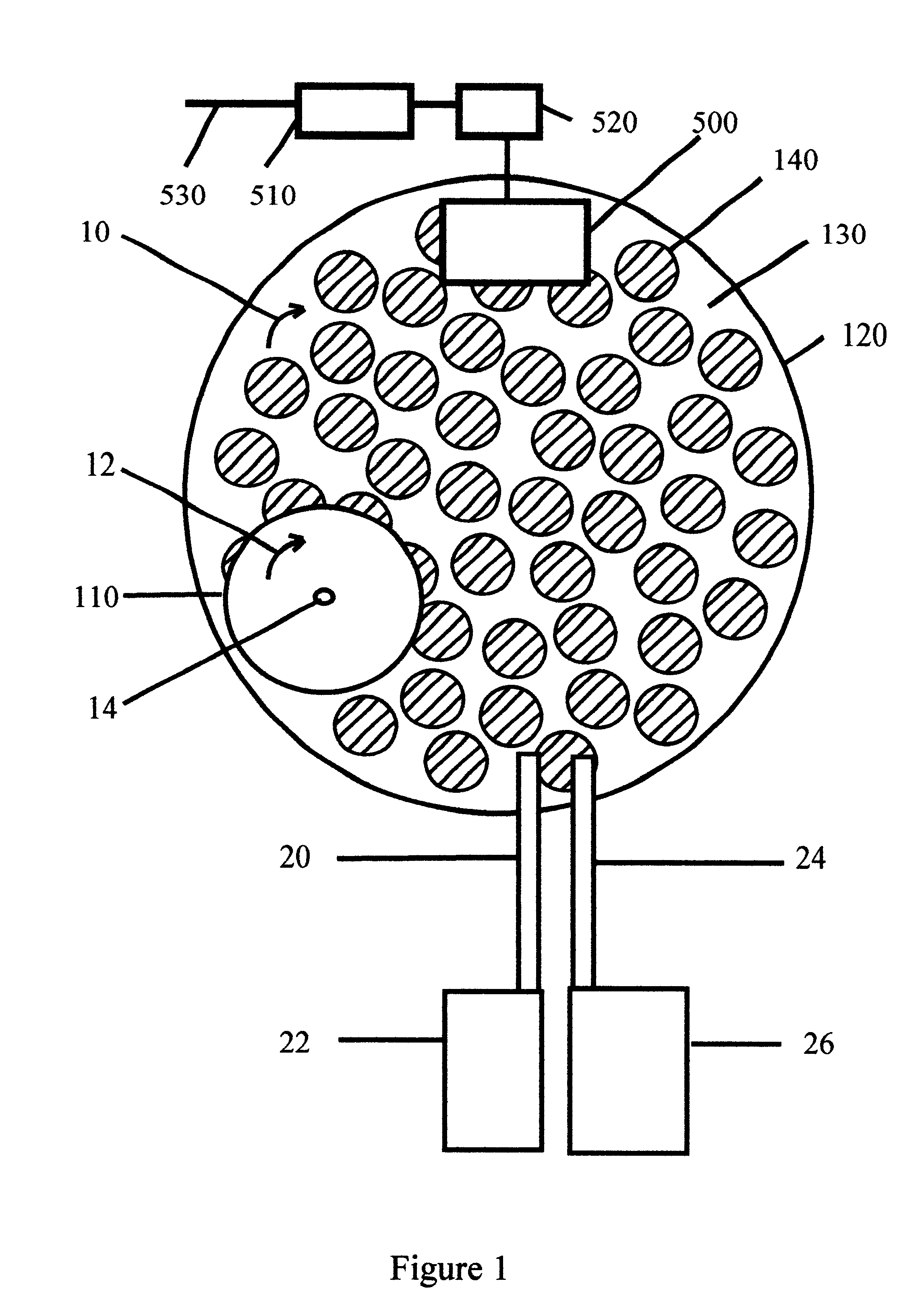
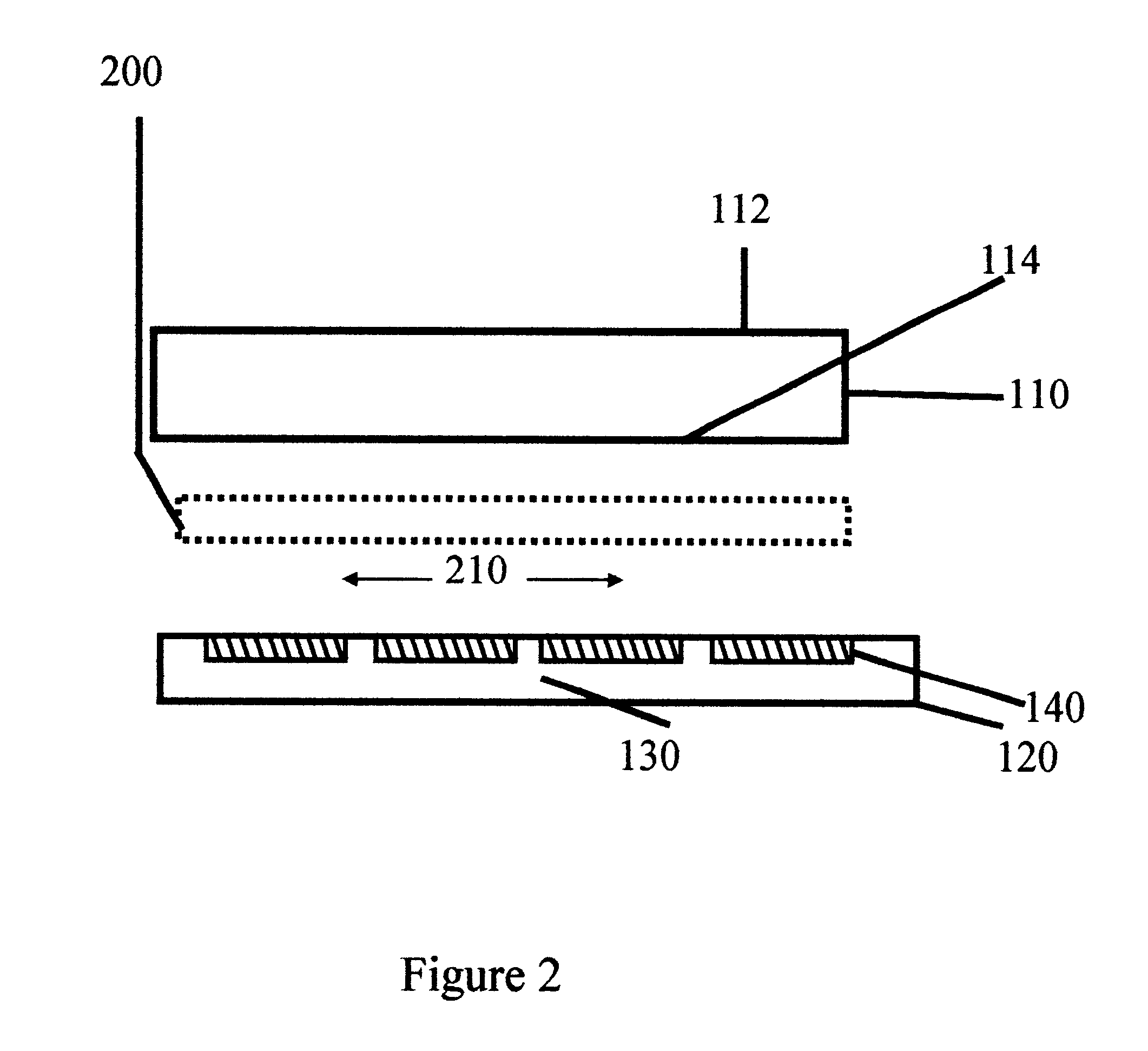
unitary finishing element is prepared. The unitary resilient body is subpad style T66541 commercially available from Fruedenberg. The subpad is a porous structure having fibers, 20 inches in diameter, and is about 0.03" thick.

A composite sheet of phenolic organic synthetic plastic reinforced with cotton fibers with a thickness of about 0.03 inches is cut into 7 / 8 inch diameter disks with a hole saw. The phenolic organic synthetic plastic is believed to have a flexural modulus of about 400,000 psi and a Rockwell M hardness of about 100. The disks are then sanded using an ordinary portable circular sander with 120 grit sand paper available commercially from the 3M Company to form a 45 degree chamfer on the edge. These disks are then used as the discrete finishing members (with the discrete finishing member finishing surface having a smaller diameter than the backside of the discrete finishing members). The backside of the discrete finishing members are sanded with emery cloth having a...


PUM

PropertyMeasurementUnit
Angleaaaaaaaaaa
Thicknessaaaaaaaaaa
Pressureaaaaaaaaaa

Abstract

New, versatile finishing surfaces are described. Unitary finishing elements having discrete finishing members attached to unitary resilient body are disclosed for finishing microdevices such as semiconductor wafers. Finishing surfaces such as discrete finishing members can be comprised of a multiphase polymeric composition. The new unitary finishing elements have lower cost to manufacture and high precision. The unitary finishing elements and finishing surfaces can reduce unwanted surface defect creation on the semiconductor wafers during finishing.

Description

BACKGROUND OF INVENTIONChemical mechanical polishing (CMP) is generally known in the art. For example U.S. Pat. No. 5,177,908 issued to Tuttle in 1993 describes a finishing element for semiconductor wafers, having a face shaped to provide a constant, or nearly constant, surface contact rate to a workpiece such as a semiconductor wafer in order to effect improved planarity of the workpiece. U.S. Pat. No. 5,234,867 to Schultz et al. issued in 1993 describes an apparatus for planarizing semiconductor wafers which in a preferred form includes a rotatable platen for polishing a surface of the semiconductor wafer and a motor for rotating the platen and a non-circular pad is mounted atop the platen to engage and polish the surface of the semiconductor wafer. Fixed abrasive finishing elements are known for polishing. Illustrative examples include U.S. Pat. No. 4,966,245 to Callinan, U.S. Pat. No. 5,823,855 to Robinson, and WO 98 / 06541 to Rutherford.An objective of polishing of semiconductor...

Claims


Application Information

Patent Timeline
IPC IPC(8): B24D7/06B24D3/34B24D3/20B24D3/28B24D7/00B24B37/04
CPCB24B37/042B24B37/245B24D3/346B24D7/063B24D3/28Y10S451/921
Inventor MOLNAR, CHARLES J.
Owner SEMCON TECH
Why Eureka
Try Eureka