Chip component assembly

a chip and component technology, applied in the field of printed circuit boards, can solve the problems of divergence in cost and performance, the average cost of computers has also declined during the same period, and the cost of computers has also declined

Inactive Publication Date: 2003-11-18
HEWLETT-PACKARD ENTERPRISE DEV LP
View PDF110 Cites 20 Cited by
  • Summary
  • Abstract
  • Description
  • Claims
  • Application Information

AI Technical Summary

Benefits of technology

The present invention has been developed in response to the current state of the art, and in particular, in response to these and other problems and needs that have not been fully or adequately resolved by currently available chip component assemblies. Thus, it is an overall object of embodiments of the present invention to provide a chip component assembly which includes an arrangement of chip components that promotes efficient use of the surface area of the PCB to which the chip component array is mounted, while also lending itself to use in conjunction with pick-and-place manufacturing processes, and which includes a grounding device that facilitates grounding of an array of chip components both to a PCB and a secondary ground plane.
Embodiments of the present invention are well suited for use in the context of PC cards and the like. However, it will be appreciated that embodiments of the present invention are suitable for use in any application or environment where it is desired to employ a chip component assembly that may be grounded to or contacting at least two different structures while at the same time maximizing the efficiency with which the surface area of a PCB is utilized, and which can be readily installed using pick-and-place manufacturing.
Due to the edge mounted, or "tombstone," orientation of the chip components, the chip component assembly is effective in promoting a relatively more efficient use of available surface area on the PCB to which it is mounted. Further, the configuration and disposition of the array ground plane and ground path structure facilitates simultaneous grounding of the chip component assembly to the PCB as well as to the ancillary ground plane. Finally, because the chip component assembly is manufactured prior to placement on the printed circuit board, it is well suited for use in conjunction with pick-and-place manufacturing techniques and thus eliminates the costs typically associated with partial or complete manual assembly and placement.
In operation, the functionality of the chip component assembly is facilitated by the connections between the respective first and second terminal elements of the chip capacitors and the electronic circuitry on the printed circuit board. Any electrostatic charge buildup, or undesirable noise, in the chip component assembly is safely drained from the chip component assembly by way of the array ground plane and ground path structure. In one embodiment of the present invention, the chip component assembly serves to provide a common AC reference between a modem in the PC card and the telephone line to which the modem is connected.

Problems solved by technology

One such factor is that while the capabilities and performance of computers have improved dramatically in recent years, the average cost of computers has also declined during the same period.
This divergence in cost and performance has been a significant factor in fueling the demand for personal computers.
Accordingly, downsizing and miniaturization of computer components is an issue of great importance in the industry.
Notwithstanding the foregoing useful features, various problems and shortcomings have conspired to impede advancement in the art.
As discussed in greater detail below however, the aforementioned chip component configurations and installation processes implicate at least one significant problem.
In view of the demand for PC cards of increasing power and functionality, and the consequent emphasis on efficient use of the limited PCB surface area, such chip placement arrangements are undesirable because they unnecessarily occupy space on the PCB that could otherwise be used to accommodate the installation of additional components.
While known chip component arrays contribute to an increase in the efficiency with which PCB space is utilized, they nevertheless suffer from a variety of problems and shortcomings.
However, because such grounding devices must connect with a plurality of components in order to effectively ground all such components, many known grounding devices are typically relatively large and bulky components that occupy a relatively large portion of space inside the PC card and accordingly serve to preclude the installation of additional components that could otherwise be employed.
Due to the relatively large size of such grounding clips, and the limited precision with which a human can manipulate and assemble small devices such as PC cards and their component parts, the grounding pad on the PCB to which the grounding device must be attached is relatively large.
The relatively large size of the grounding pad required by the grounding device acts as yet another limitation on the available space on the PCB and, accordingly, the efficiency with which such space is used.
Another problem associated with such known arrangements concerns associated manufacturing processes.
In particular, such chip component array and grounding device arrangements typically implicate at least two installation steps.
However, because the grounding device is separate from the chip component array, an additional step is required to attach the grounding device to the chip component array and the PCB.
As noted above, the inefficiency of the manufacturing process is further aggravated by the face that the grounding device typically is not placed by a machine but rather must be placed manually on the PCB.
Note that in situations where a chip component array is not employed, the efficiency of the assembly process is further impaired.
Such processes tend to impair both the speed and the quality associated with the manufacturing of the PC card and accordingly contribute to an increase in the overall cost of the PC card.
However, the use of two grounding devices complicates the PC card assembly process and accordingly contributes to an overall increase in the cost of the PC card.

Method used


Image

  • Chip component assembly
  • Chip component assembly
  • Chip component assembly

Examples


Embodiment Construction

Reference will now be made to figures wherein like structures will be provided with like reference designations. It is to be understood that the drawings are diagrammatic and schematic representations of various embodiments of the claimed invention, and are not to be construed as limiting the present claimed invention, nor are the drawings necessarily drawn to scale.

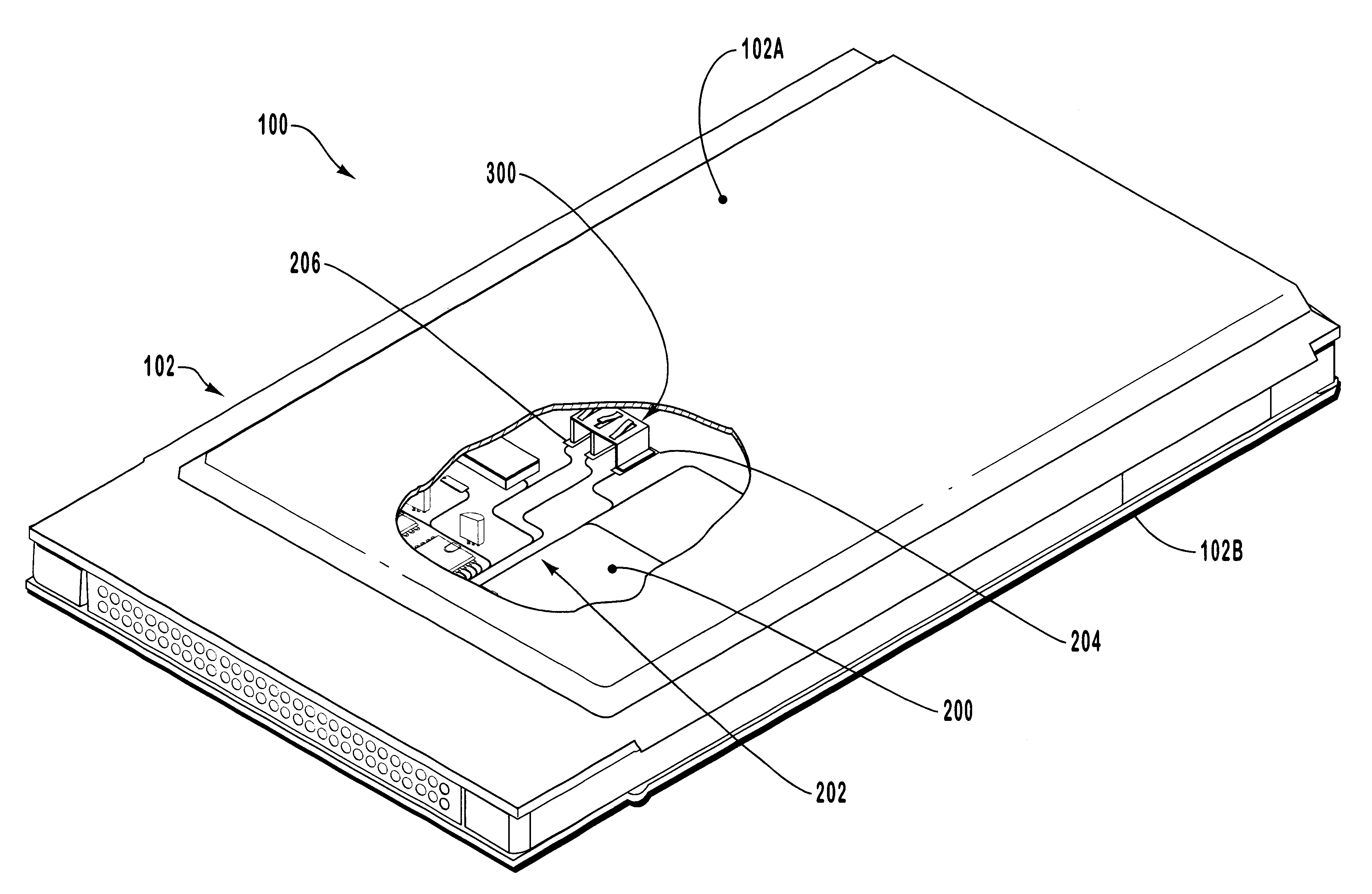
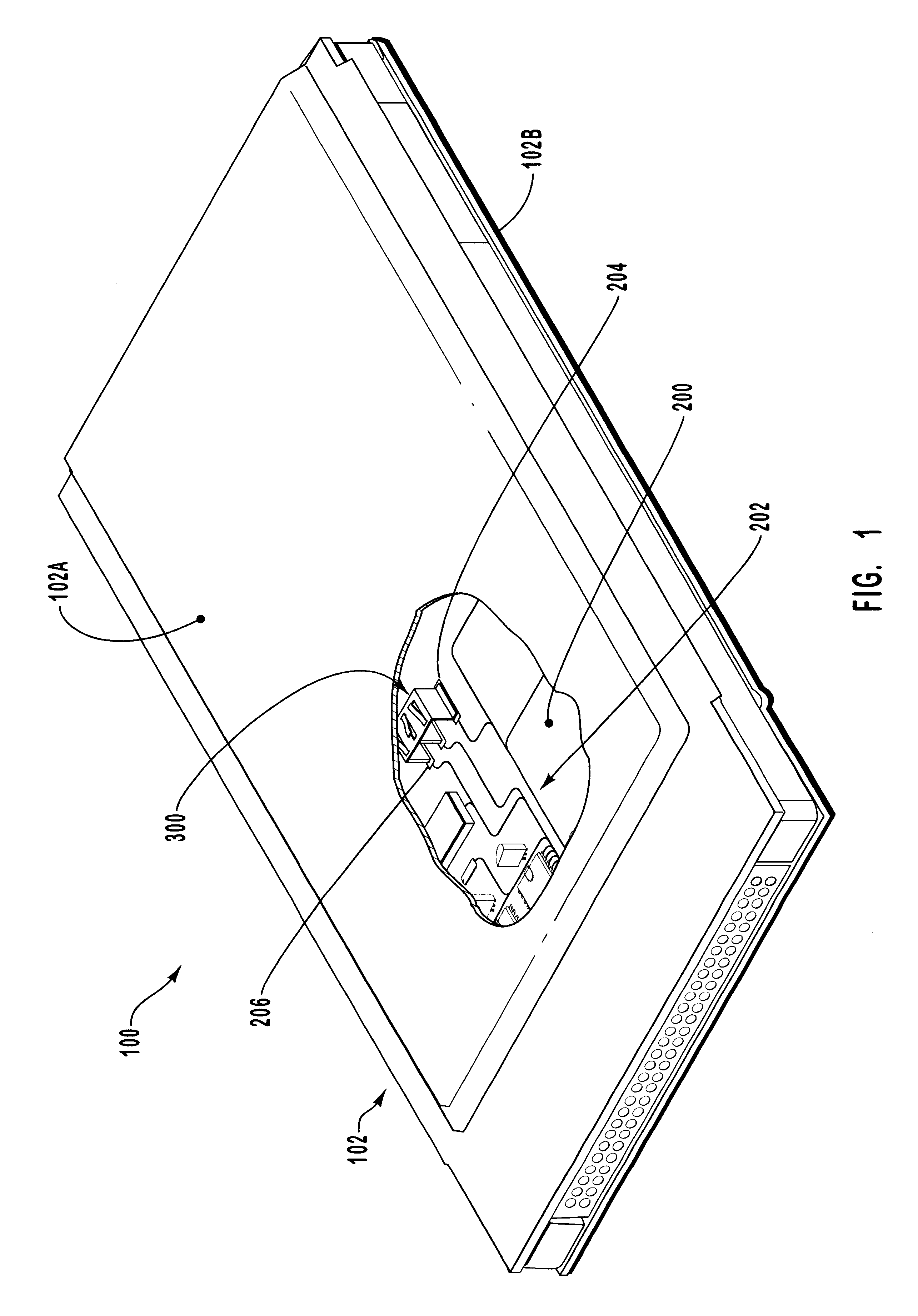
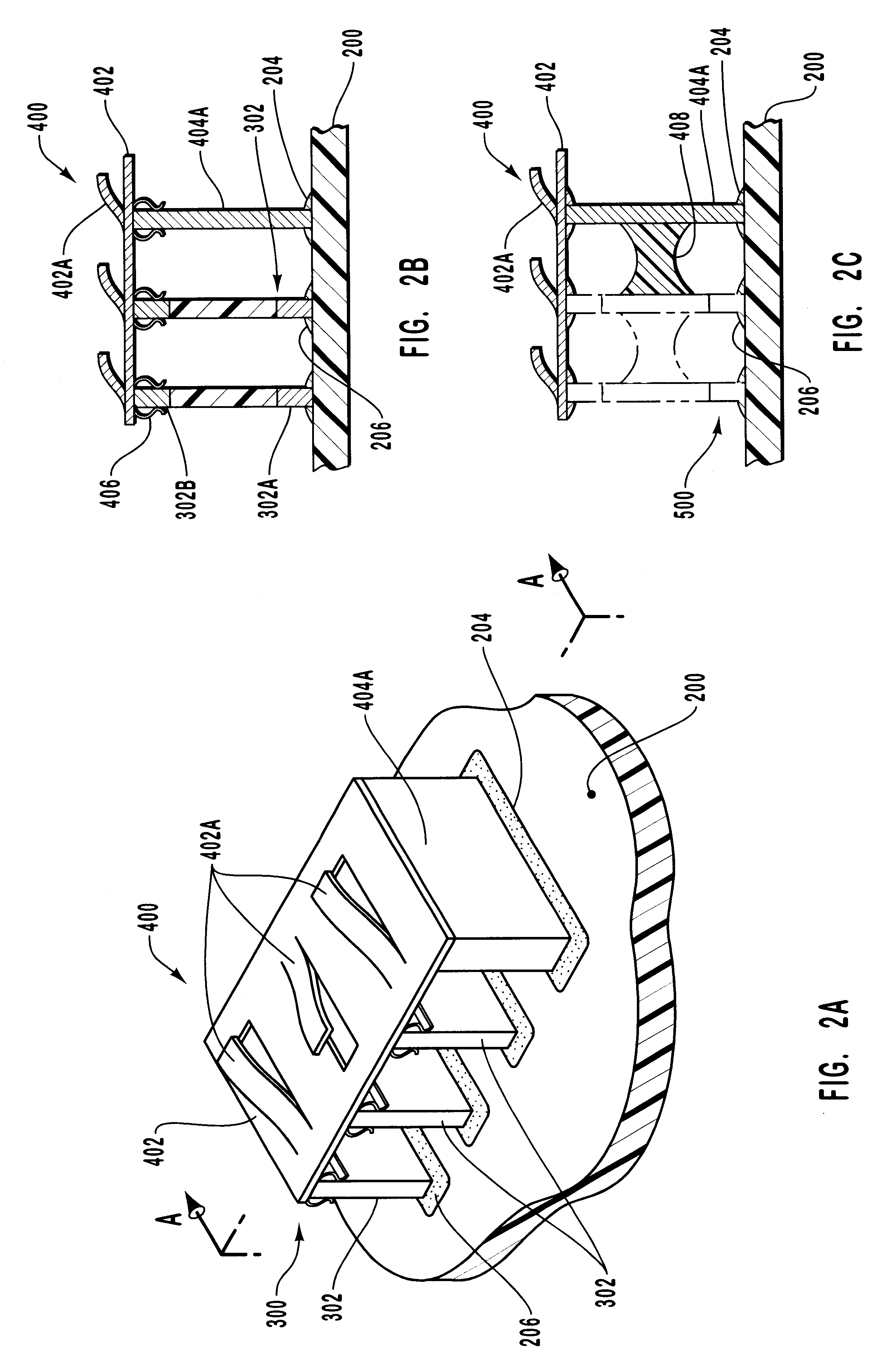
Reference is first made to FIG. 1, wherein a PC card is indicated generally at 100. It will be appreciated that PC card may take any of a variety of forms including, but not limited to, a memory card, modem card, network card, or the like. It will likewise be appreciated that PC card 100 is an exemplary operating environment, and that embodiments of the present invention may be profitably employed in a wide variety of other environments as well. In general, embodiments of the present invention are suitable for use in any environment where printed circuit boards (PCB) are employed.

In the illustrated embodiment, PC card 10...


PUM


Abstract

A chip component assembly is provided that includes a plurality of chip components each having respective first and second terminal elements, the first terminal elements being joined to corresponding solder pads on a printed circuit board, the solder pads being in communication with electronic circuitry of the printed circuit board, and the second terminal elements being joined together by an array ground plane of a grounding device. The grounding device additionally includes a ground path structure which physically and electrically connects the array ground plane, and thus the chip components, to a ground pad located on the printed circuit board so as to provide a ground path from the chip components. Preferably, the array ground plane additionally includes a plurality of resilient contact elements which provide for substantial and continuous contact between the array ground plane and an ancillary ground plane, such as the top cover of a PC card. The grounding device serves to foreclose electrostatic discharge or EMI by the chip components and in some applications further serves to direct undesirable noise to ground. The relatively small size of the grounding device permits the use of a relatively smaller ground pad on the printed circuit board, thereby conserving valuable printed circuit board surface area. Finally, the ground path structure is configured for automated attachment to the chip components, and the chip component assembly thus formed is well suited for installation on the printed circuit board by pick-and-place manufacturing techniques.

Description

1. The Field of the InventionThe present invention relates generally to printed circuit boards for use in PC cards. More particularly, embodiments of the present invention relate to an improved chip component assembly which streamlines the manufacturing of the PC card while also utilizing relatively less space on the printed circuit board.2. The Relevant TechnologyThe ever-increasing demand for personal computers and related equipment may be ascribed to any of a variety of factors. One such factor is that while the capabilities and performance of computers have improved dramatically in recent years, the average cost of computers has also declined during the same period. This divergence in cost and performance has been a significant factor in fueling the demand for personal computers.Another factor driving the demand for personal computers is the expansion and development of the global computer network commonly known as the "Internet," and related network communications. More and mor...

Claims


Application Information

Patent Timeline
Patent Type & Authority Patents(United States)
IPC IPC(8): H05K5/02H05K9/00H05K1/02
CPCH05K1/0231H05K5/0256H05K9/0039H05K2201/10636H05K2201/10371H05K2201/10492Y02P70/50
Inventor NELSON, JON A.GILES, RICKOLIPHANT, DAVID
Owner HEWLETT-PACKARD ENTERPRISE DEV LP
Why Eureka
Try Eureka