Enhanced deposition control in fabricating devices in a semiconductor wafer

a technology of enhanced deposition control and fabricating device, which is applied in the direction of semiconductor devices, chemical vapor deposition coatings, coatings, etc., can solve the problems of continuous shrinkage of device and circuit features

Inactive Publication Date: 2003-12-02
NEC ELECTRONICS CORP
View PDF13 Cites 88 Cited by
  • Summary
  • Abstract
  • Description
  • Claims
  • Application Information

AI Technical Summary

Benefits of technology

An object of the present invention is to provide a method for enhanced deposition control over the prior art deposition techniques of silicon nitride layer in terms of time and / or improving electron mobility within underlying structure.

Problems solved by technology

The drive toward this ultra large-scale integration has resulted in continued shrinking of device and circuit features.

Method used


Image

  • Enhanced deposition control in fabricating devices in a semiconductor wafer
  • Enhanced deposition control in fabricating devices in a semiconductor wafer
  • Enhanced deposition control in fabricating devices in a semiconductor wafer

Examples


Embodiment Construction

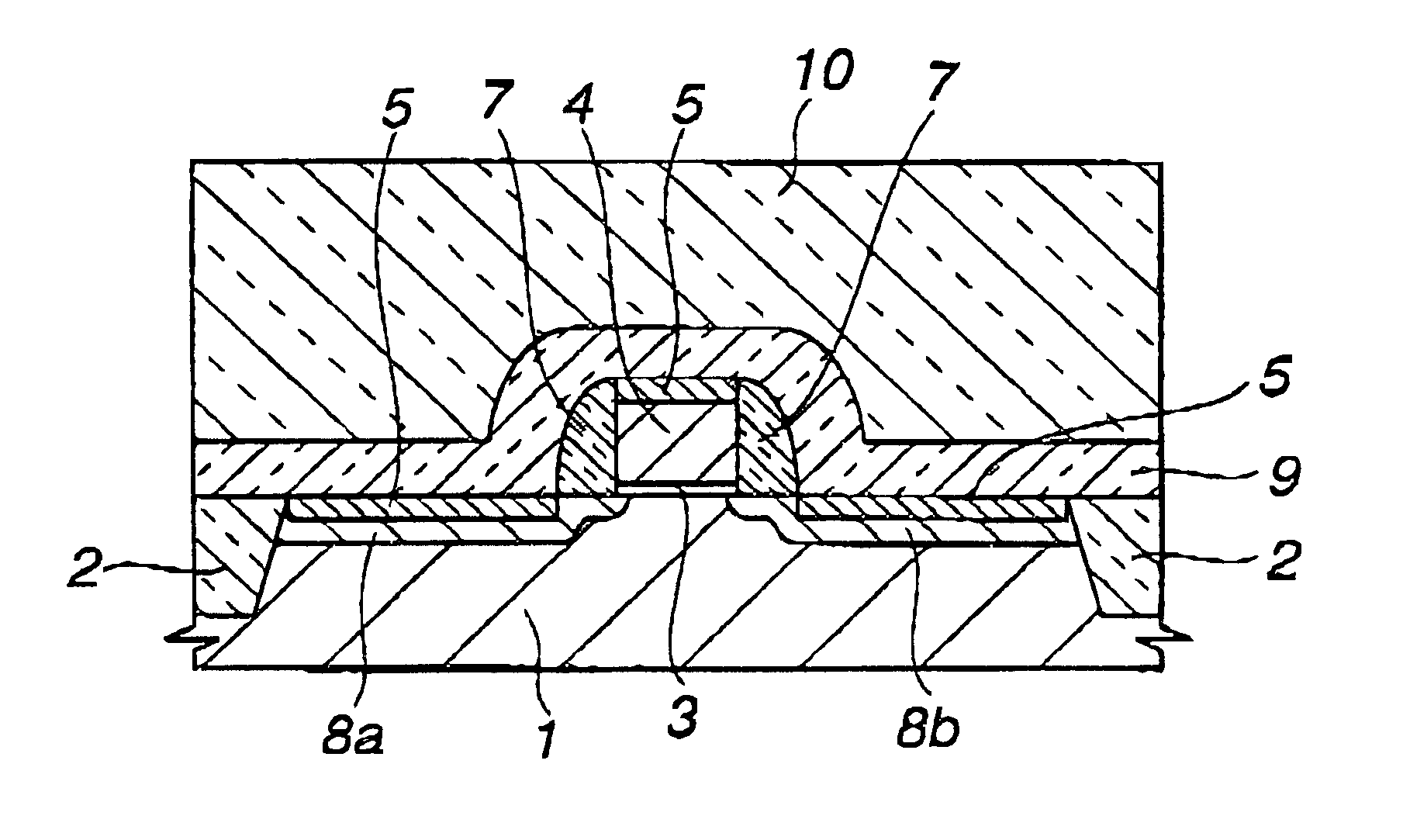
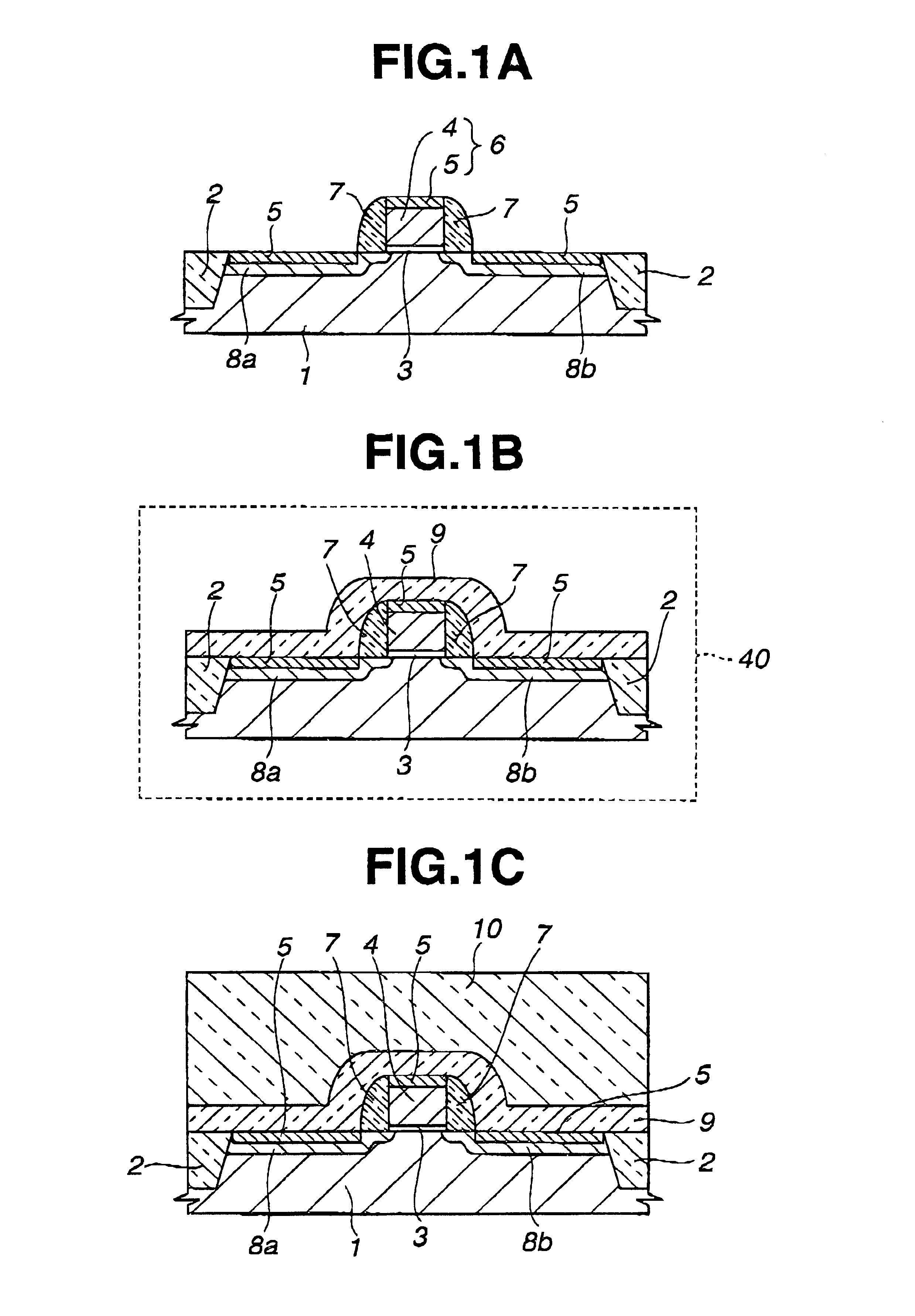
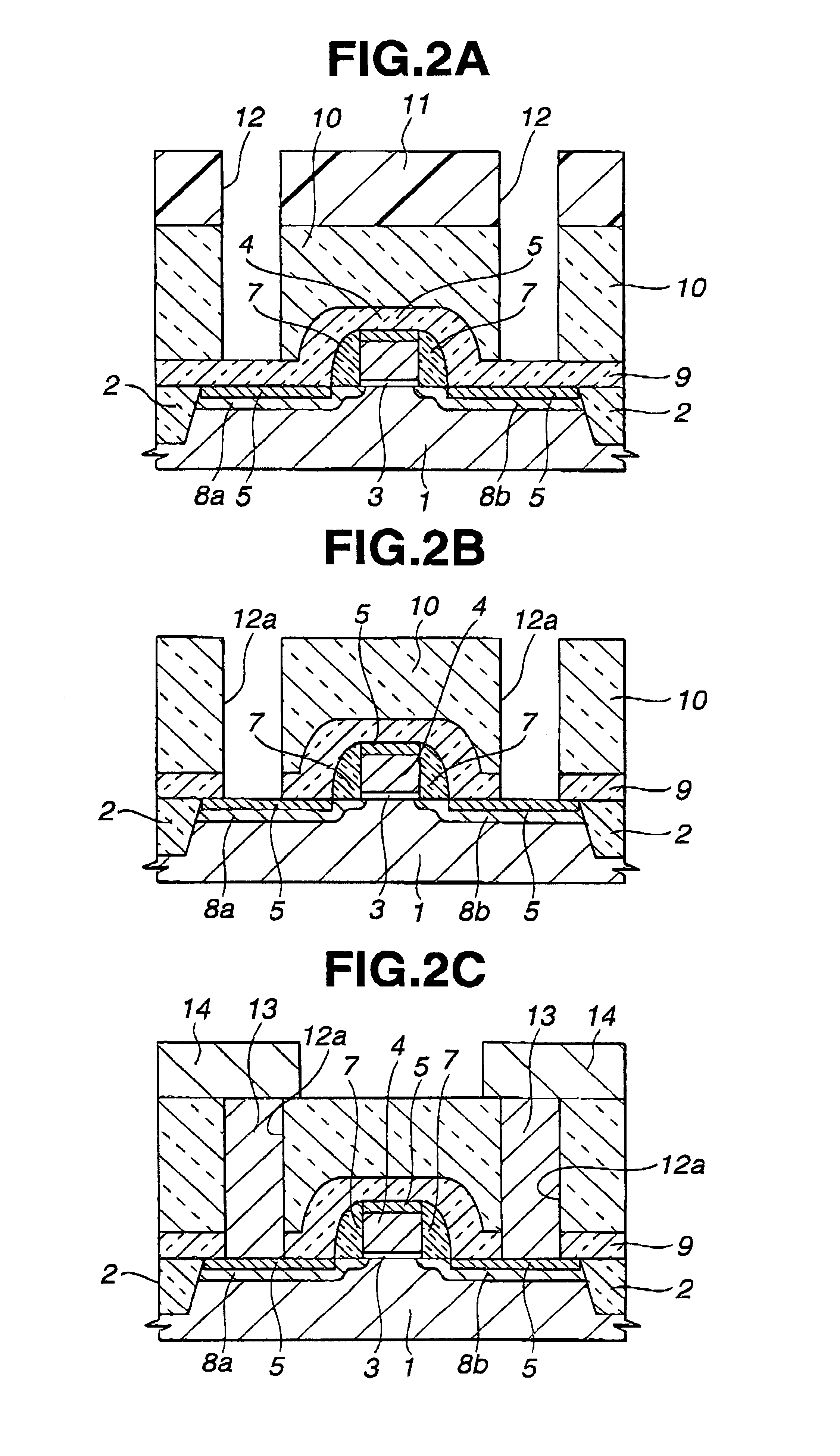
The process steps and structures described below do not form a complete process flow for fabricating integrated circuits in a semiconductor wafer. The present invention can be practiced in conjunction with integrated circuit fabrication techniques currently used in the art, and only so much of the commonly practiced process steps are included as are necessary for an understanding of the present invention. The figures representing cross sections of portions of a device during fabrication are not drawn to scale, but instead are drawn to illustrate the features of the present invention.

In accordance with an exemplary embodiment of the present invention, there is provided an enhanced deposition process for use in fabricating a dual-layer dielectric in a manner to improve performance of the underlying device or devices. The dual-layer dielectric includes a silicon nitride layer 9 and an overlying dielectric layer 10 (see FIG. 1C). For example, the dual-layer dielectric includes a thick d...


PUM

PropertyMeasurementUnit
temperatureaaaaaaaaaa
pressureaaaaaaaaaa
temperatureaaaaaaaaaa

Abstract

A method for an enhanced deposition control includes forming a transistor on a substrate of a semiconductor wafer, and depositing a silicon nitride layer on the transistor and the substrate in a reactor at a pressure of at least approximately 10<4 >Pa.

Description

1. Field of the InventionThe present invention relates to a method for an enhanced deposition control in fabricating devices in a semiconductor wafer.2. Description of the Related ArtA continuing trend in semiconductor technology is to build integrated circuits with more and / or faster semiconductor devices. The drive toward this ultra large-scale integration has resulted in continued shrinking of device and circuit features. Among such trend, fabrication of semiconductor devices involves deposition of a silicon nitride layer over a semiconductor wafer to protect underlying structure.Various deposition techniques of a silicon nitride layer are known. One such technique is disclosed in U.S. Pat. No. 6,060,393 wherein a silicon oxynitride layer is deposited using plasma enhanced chemical vapor deposition (PECVD) process and used as an etch-stop layer for a local interconnect. Another technique is disclosed in U.S. Pat. No. 5,997,757 wherein a silicon nitride layer is deposited using lo...

Claims


Application Information

Patent Timeline
Patent Type & Authority Patents(United States)
IPC IPC(8): C23C16/34H01L21/02H01L21/768H01L21/70H01L21/318H01L21/60H01L21/8234H01L29/78H01L21/20
CPCC23C16/345H01L21/3185H01L21/76801H01L21/76802H01L29/7843H01L21/76895H01L21/76897H01L21/823425H01L21/823475H01L21/76834H01L21/02274H01L21/0217H01L21/20
Inventor ITO, SHINYA
Owner NEC ELECTRONICS CORP
Why Eureka
Try Eureka