Solid state transmitter circuit

a transmitter circuit and solid-state technology, applied in the direction of instruments, amplifiers with semiconductor devices/discharge tubes, antennas, etc., can solve the problems of n levels of combining, increased size and cost, and replacement of vacuum tube systems with high-power solid-state systems

Inactive Publication Date: 2004-01-13
RAYTHEON CO
View PDF5 Cites 3 Cited by
  • Summary
  • Abstract
  • Description
  • Claims
  • Application Information

AI Technical Summary

Problems solved by technology

However, considerations including ohmic feed losses, size and costs have discouraged replacing vacuum tube systems with high power solid state systems at microwave frequencies.
In particular, high power solid state microwave systems built with poor efficiency increases solid state device counts which resulted in increased size and cost.
The drawback of the corporate waveguide feed is that for 2.sup.N modules typically there need to be N levels of combining.
The design for a radial combiner can be difficult in terms of impedance match, and also the orientation may not lend itself adaptable for cooling modules.
A drawback for prior attempts using traveling wave feeds has been that a larger number of ports (e.g., up to 50) usually have been necessary for better efficiency.
Design, manufacturing and maintenance of solid state subarray power blocks is sometimes difficult to achieve using state of the art combining techniques.

Method used


Image

  • Solid state transmitter circuit
  • Solid state transmitter circuit
  • Solid state transmitter circuit

Examples


Embodiment Construction

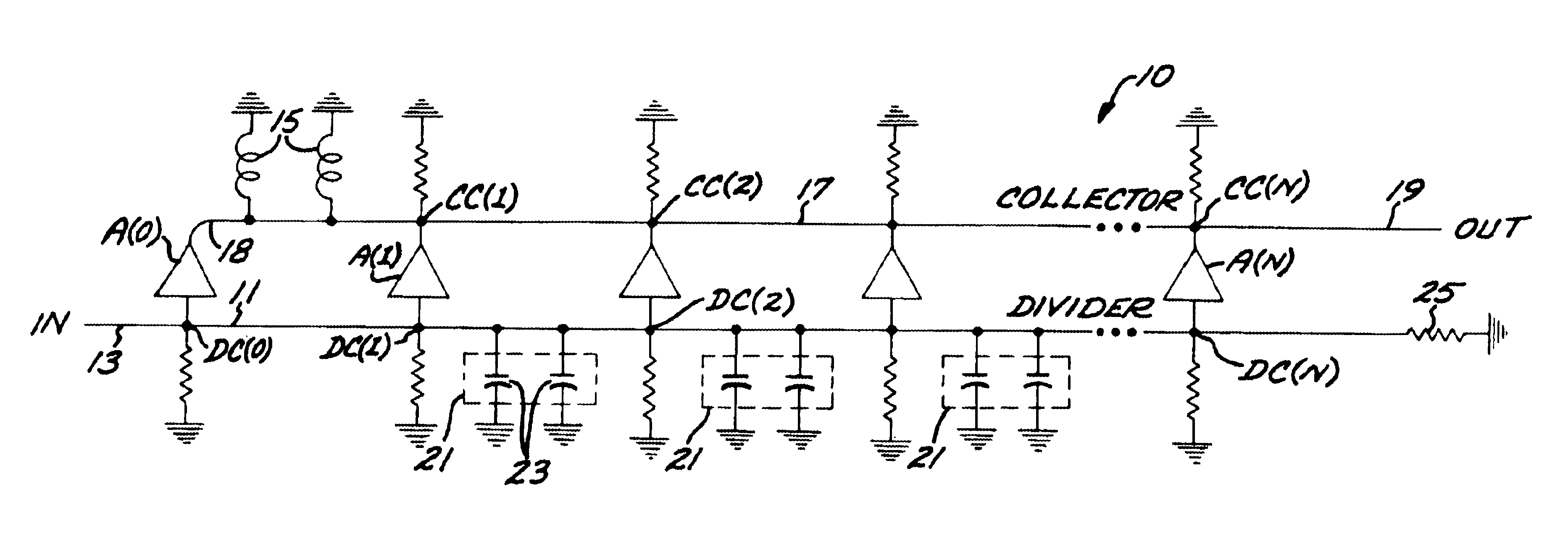
FIG. 1 is a schematic electrical diagram of elements of a solid state transmitter circuit 10 that employs features of the invention. The transmitter circuit 10 includes a divider series feed signal line or path 11 that receives an RF signal at an input or start 13 which is the input to the combiner circuit. The divider series feed signal path 11 can comprise a suitable microwave transmission line such as a waveguide. Respective divider directional couplers DC(0)-DC(N) are connected to the divider series feed signal line 11 at a spacing of about one half of a selected operational wavelength, typically for waveguide transmission lines, but not necessarily, particularly for applications using other transmission media, at the center of an operating frequency band. The 0.sup.th directional coupler DC(0) is located close to or at the input 13 of the divider feed line 11. The divider directional couplers DC(0)-DC(N) are configured to couple power from the divider feed line 11 to respective...


PUM


Abstract

A microwave transmitter circuit including a divider series feed signal line, collector series feed signal line, a plurality of parallel solid state amplifier coupler circuits connected between the divider series feed line and the collector series feed line, and phase shifting circuitry distributed along the collector series feed line for compensating phase tracking error between the divider series feed line and the collector series feed line.

Description

TECHNICAL FIELD OF THE DISCLOSUREThis invention relates to active transmitter circuits for radar systems.BACKGROUND OF THE DISCLOSURERadar or communications systems including an active transmitter module coupled to a passive array antenna or sub-array could benefit with an efficient feed network that enables solid state combining. Generic solid state devices have been shown to be more functional, reliable, compact, easily upgraded and lower cost compared to the maintenance of tube based systems.However, considerations including ohmic feed losses, size and costs have discouraged replacing vacuum tube systems with high power solid state systems at microwave frequencies. In particular, high power solid state microwave systems built with poor efficiency increases solid state device counts which resulted in increased size and cost. The new technique for combining solid state devices as disclosed herein achieves cost and size competitiveness and offers improved performance compared to vac...

Claims


Application Information

Patent Timeline
Patent Type & Authority Patents(United States)
IPC IPC(8): H01P5/16H01P5/18H03F3/60
CPCH01P5/181H03F3/605H01P1/18H03F3/60H01P5/18
Inventor LIVINGSTON, STAN W.
Owner RAYTHEON CO
Why Eureka
Try Eureka