Triple slope pixel sensor and arry

a pixel sensor and triple slope technology, applied in the field ofmos active pixel sensors, can solve the problems of limitation of the dynamic range of images that can be captured by the array, and the technique is not applicable to the cmos sensor array

Inactive Publication Date: 2004-02-24
FOVEON
View PDF106 Cites 47 Cited by
  • Summary
  • Abstract
  • Description
  • Claims
  • Application Information

AI Technical Summary

Problems solved by technology

In the CCD art, techniques have been developed for preventing leakage and contamination due to minority carrier diffusion and leakage, but these techniques are not applicable to the CMOS senso

Method used


Image

  • Triple slope pixel sensor and arry
  • Triple slope pixel sensor and arry
  • Triple slope pixel sensor and arry

Examples


Embodiment Construction

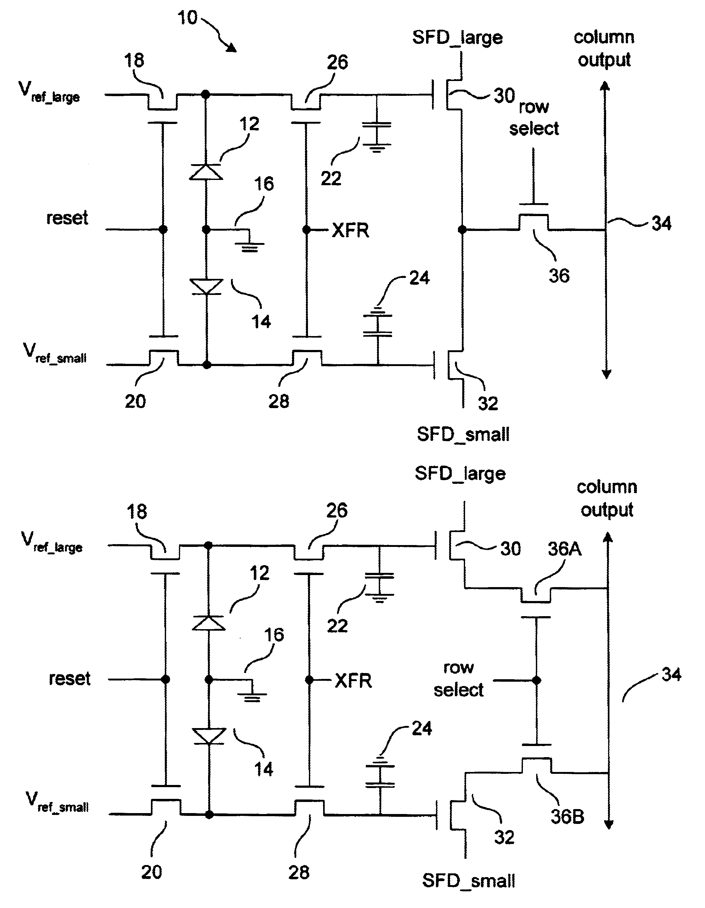
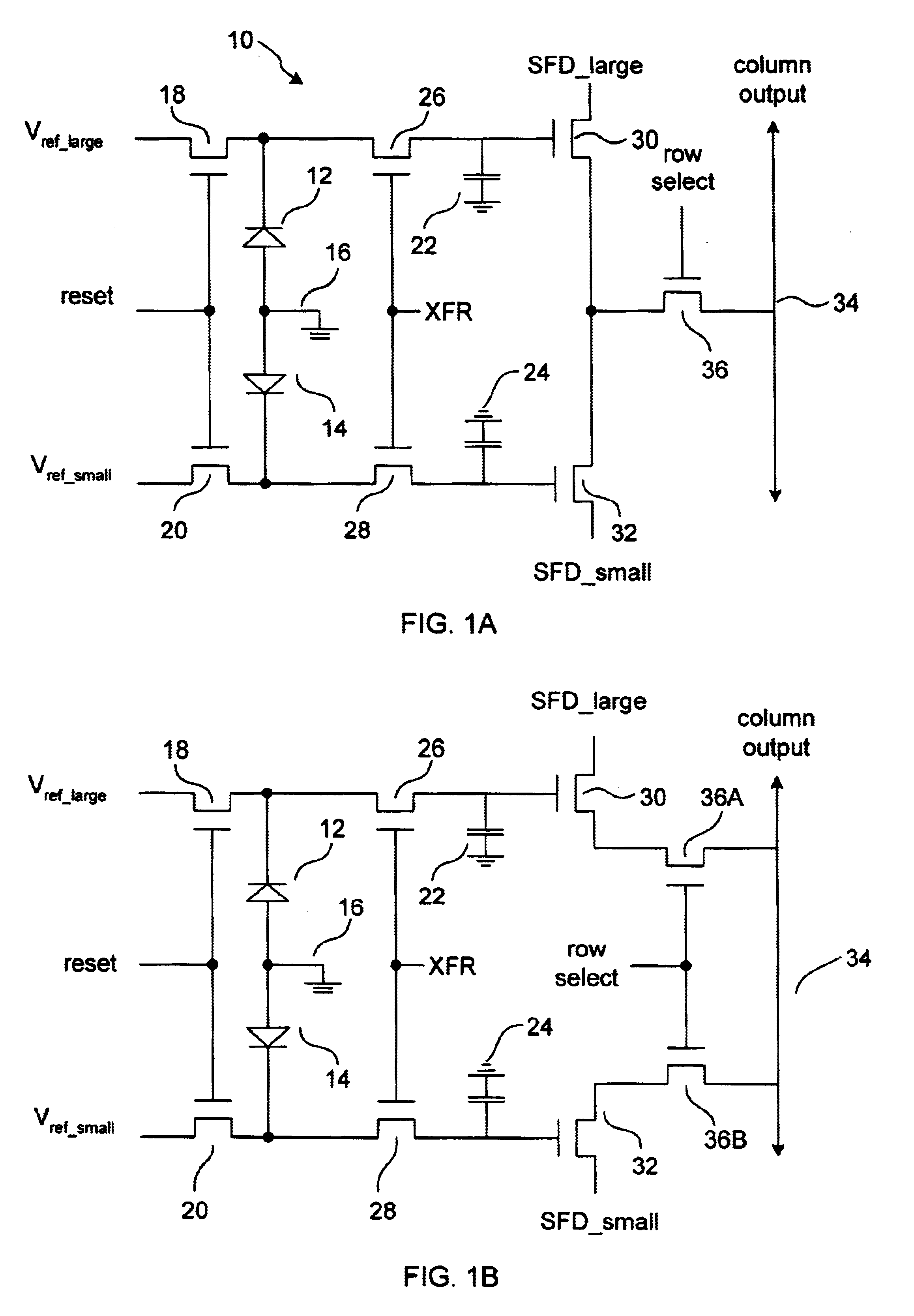
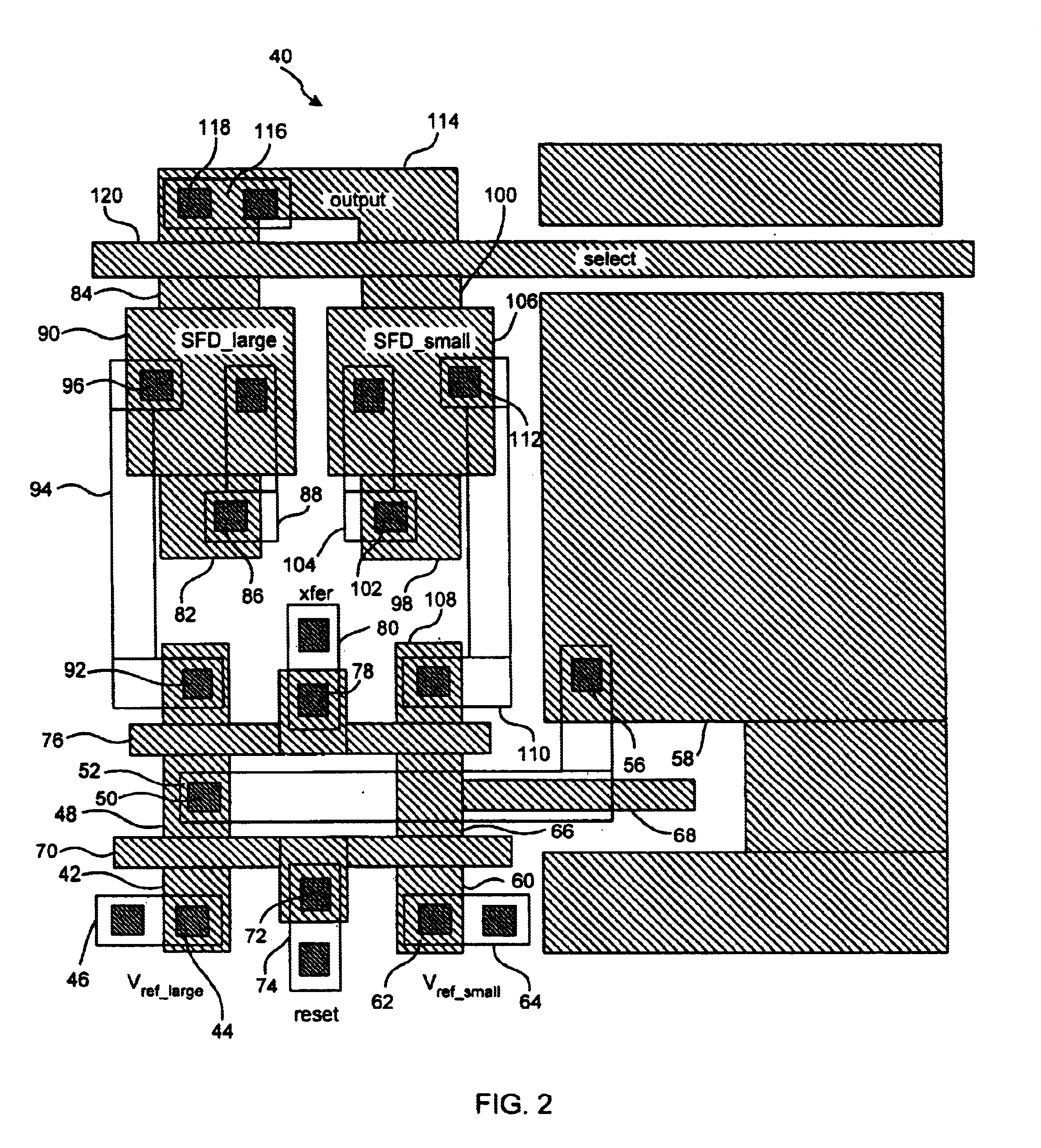
Persons of ordinary skill in the art will realize that the following description of the present invention is illustrative only and not in any way limiting. Other embodiments of the invention will readily suggest themselves to such skilled persons having the benefit of this disclosure. For example, the illustrative embodiments of the present invention are disclosed using all N-Channel MOS transistor switches, but other technologies could be employed as well.

Referring first to FIG. 1A, a schematic diagram of an illustrative embodiment of a triple-slope MOS active pixel sensor 10 according to the present invention is shown. First and second photodiodes 12 and 14, respectively, are shown having their anodes connected to ground potential at reference numeral 16. Photodiode 12 is larger than photodiode 14. Typically, photodiode 12 may be about 10 square microns and photodiode 14 may be less than one square micron.

The cathode of photodiode 12 is connected to the source of N-Channel MOS Res...


PUM


Abstract

A triple-slope MOS active pixel sensor disposed on a semiconductor substrate comprises first and second capacitive storage elements each having a first terminal connected to a fixed potential and a second terminal. First and second photodiodes each have a first terminal connected to a fixed potential and a second terminal. The second photodiode is smaller than the first photodiode. First and second semiconductor reset switches each have a first terminal connected respectively to the second terminal of the first and second photodiodes and a second terminal connected respectively to first and second reset potentials that reverse bias the photodiodes. First and second semiconductor transfer switches each have a first terminal connected respectively to the second terminals of the first photodiode and a second terminal connected respectively to the second terminals of the first and second capacitive storage elements. First and second semiconductor amplifiers each have an input connected respectively to the second terminals of the first and second capacitive storage elements and have their outputs connected together. The first and second semiconductor reset switches and the first and second semiconductor transfer switches each have a control element connected to a control circuit for selectively activating the first and second semiconductor reset switches and the first and second semiconductor transfer switches.

Description

1. Field of the InventionThe present invention relates to MOS active pixel sensors. More particularly, the present invention relates to a MOS active pixel sensor having a triple slope light-to-output-voltage transfer gain characteristic.2. The Prior ArtIntegrated image sensors are known in the art. Such sensors have been fabricated from charge-coupled devices (CCDs) and as bipolar and MOS image sensors.In the CCD imager art, on-chip frame storage capability has been employed previously. It has been motivated by the need to shift sensed charges out during a video frame time without letting them be contaminated by further exposure as the charges travel across the CCD array. Two storage techniques are commonly employed in the CCD imager art. According to the first technique, a second separate on-chip CCD array is provided under a light shield, and the entire image is quickly shifted along one dimension into the storage array, since shifting in one dimension is fast enough to avoid sign...

Claims


Application Information

Patent Timeline
IPC IPC(8): H04N3/15H04N5/355H04N5/374
CPCH04N3/155H04N5/35518H04N5/35509H04N25/571H04N25/573
Inventor MERRILL, RICHARD B.
Owner FOVEON
Why Eureka
Try Eureka