

Pin grid array integrated circuit connecting device
a technology of integrated circuits and connecting devices, which is applied in the direction of connection of coupling devices, connection contact member materials, electrical apparatus construction details, etc., can solve the problems of occupying a large space for pulling parts of sockets, requiring expensive integrated circuit package devices, and no extra function provided
- Summary
- Abstract
- Description
- Claims
- Application Information
AI Technical Summary
Benefits of technology
Problems solved by technology
Method used
Image

Examples
Embodiment Construction
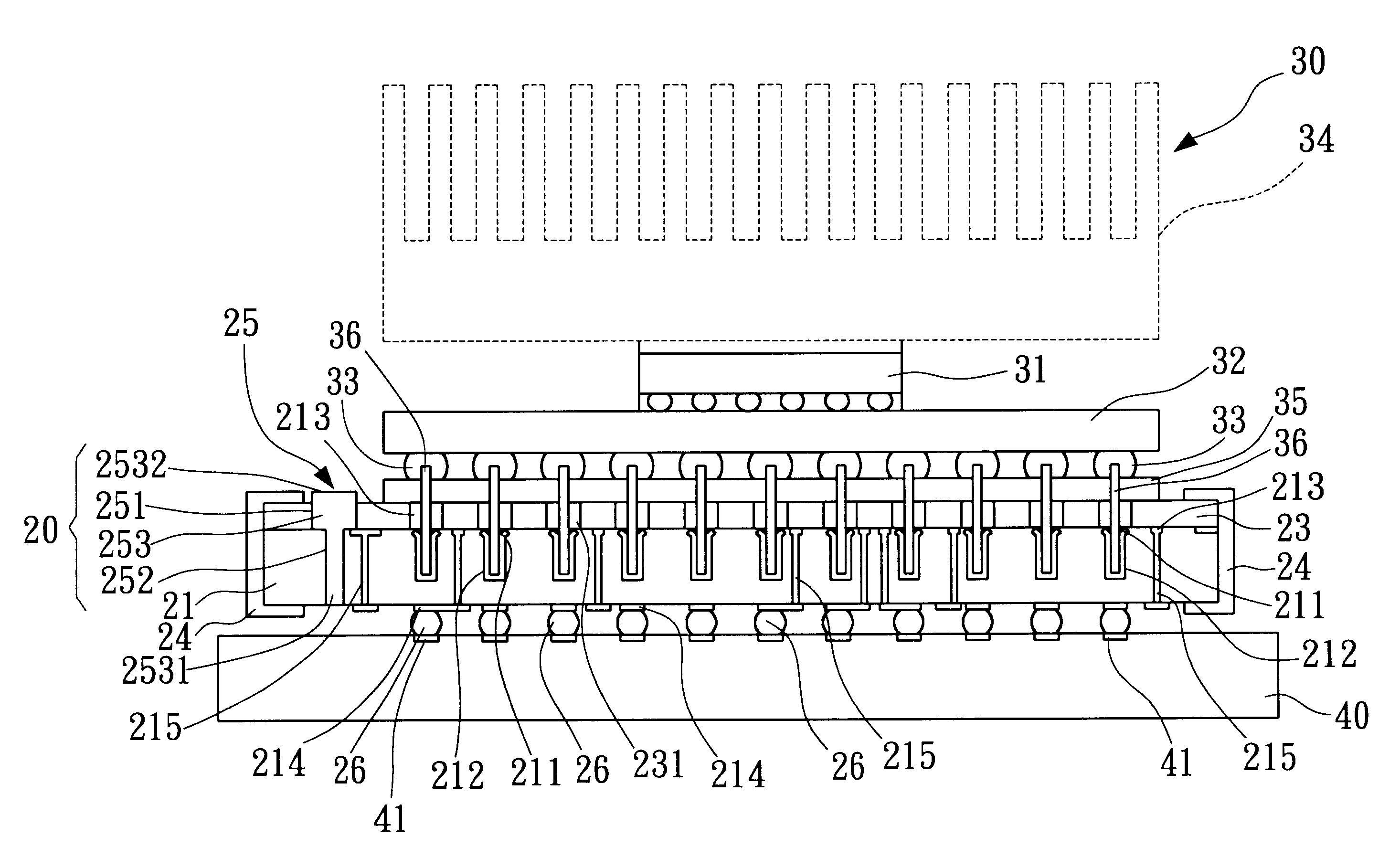
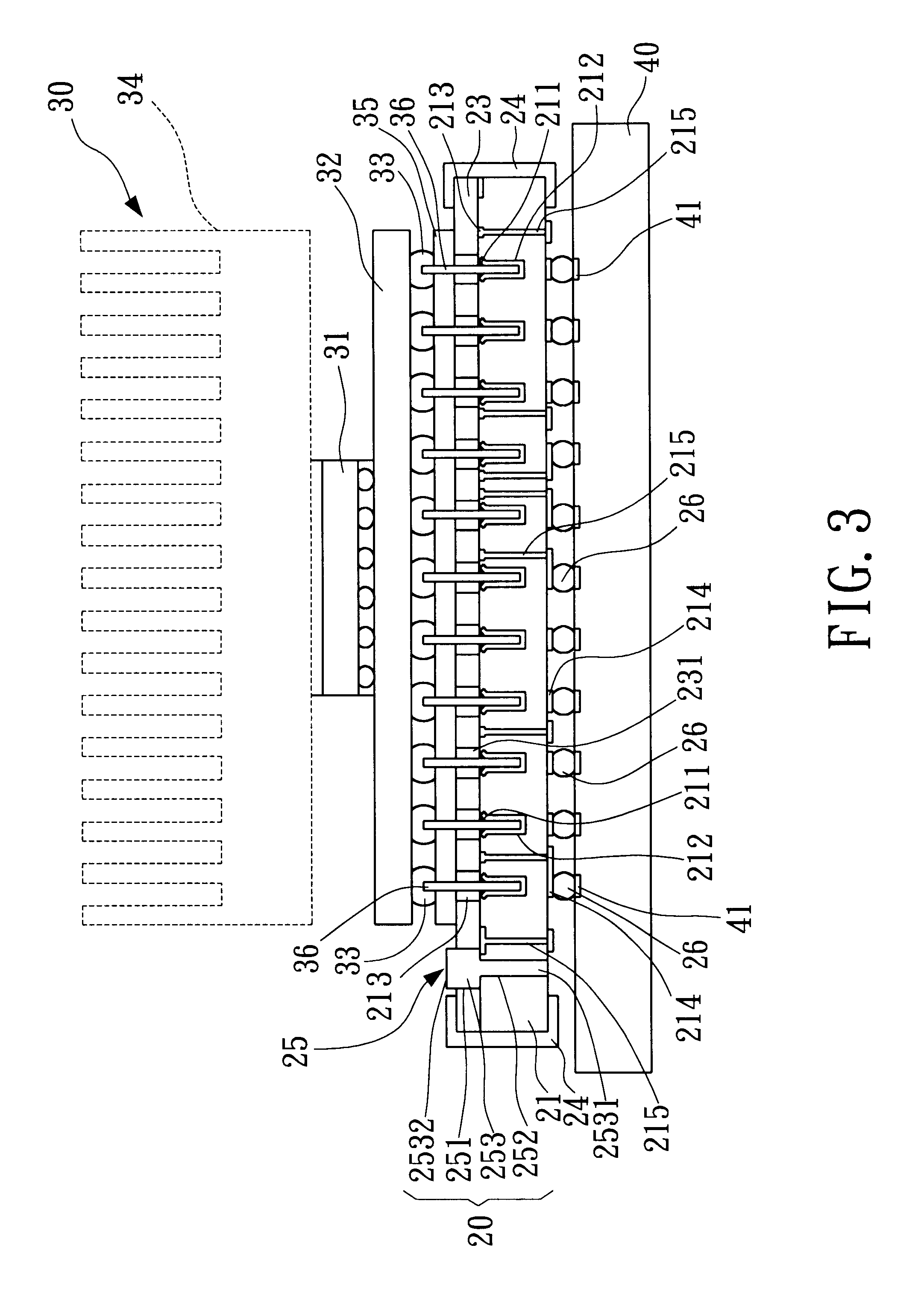
The present invention relates to a pin grid array integrated circuit connecting device. Especially, the present invention relates to a pin grid array integrated circuit connecting device which is featured with plural pin holes on a substrate to replace the plastic socket base in prior art, and some extra electronic components and circuit layout can be placed on the substrate to provide additional function. More over, a driving apparatus that can rotate horizontally will be placed to move the sliding slice linearly on the top of the substrate, which replace the pulling part used in prior art and save much space.
The following embodiments will illustrate detail information of the operation, the method, the effect of the pin grid array integrated circuit connecting device of the present invention.
In order to explain more detail about the features and the embodiment of the present invention, the follows will introduce a couple of embodiments of the pin grid array integrated circuit conne...
PUM
 Abstract
Description
Claims
Application Information