Circuit carrier and fabrication method thereof

a technology of circuit carrier and fabrication method, which is applied in the direction of sustainable manufacturing/processing, final product manufacturing, non-metallic protective coating application, etc., can solve the problems of reducing the yield of manufacturing electrical packages, and achieve the effect of enhancing the yield of manufacturing pga packages

Active Publication Date: 2006-09-05
VIA TECH INC
View PDF3 Cites 5 Cited by
  • Summary
  • Abstract
  • Description
  • Claims
  • Application Information

AI Technical Summary

Benefits of technology

[0009]Accordingly, the present invention provides a circuit carrier and a fabrication thereof adapted for a pin grid array (PGA) package. By integrating the circuit carrier and the fabrication process in the PGA package process, the yield of manufacturing PGA package is enhanced.
[0010]The present invention also provides an electrical package and a fabrication method thereof adapted for a PGA package for maintaining the yield of manufacturing the PGA package.
[0015]According to the circuit carrier and the fabrication method thereof, the fixing layer is formed over the surface of the substrate, covering the solder layer and the portion of the side surface of the pin. When the process temperature, such as reflow temperature, or operational temperature of the circuit carrier is higher than the melting point of the solder layer, the pin is still fixed to the pin pad even if the solder layer melts and cannot fix the pin. The fixing layer can avoid the shift or disposition of the pin. With the fixing layer, the yield of manufacturing the circuit carrier of the PGA package is improved.

Problems solved by technology

As a result, the yield of manufacturing the electrical package declines.

Method used


Image

  • Circuit carrier and fabrication method thereof
  • Circuit carrier and fabrication method thereof
  • Circuit carrier and fabrication method thereof

Examples


Embodiment Construction

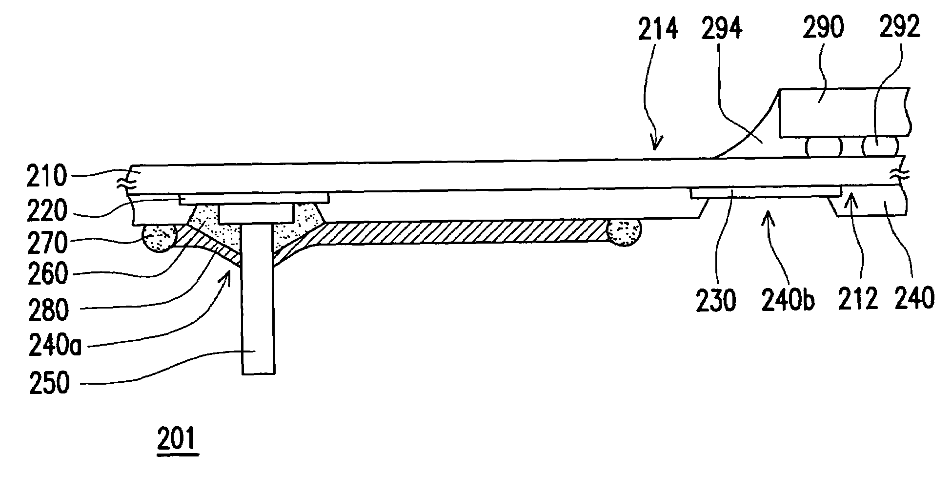
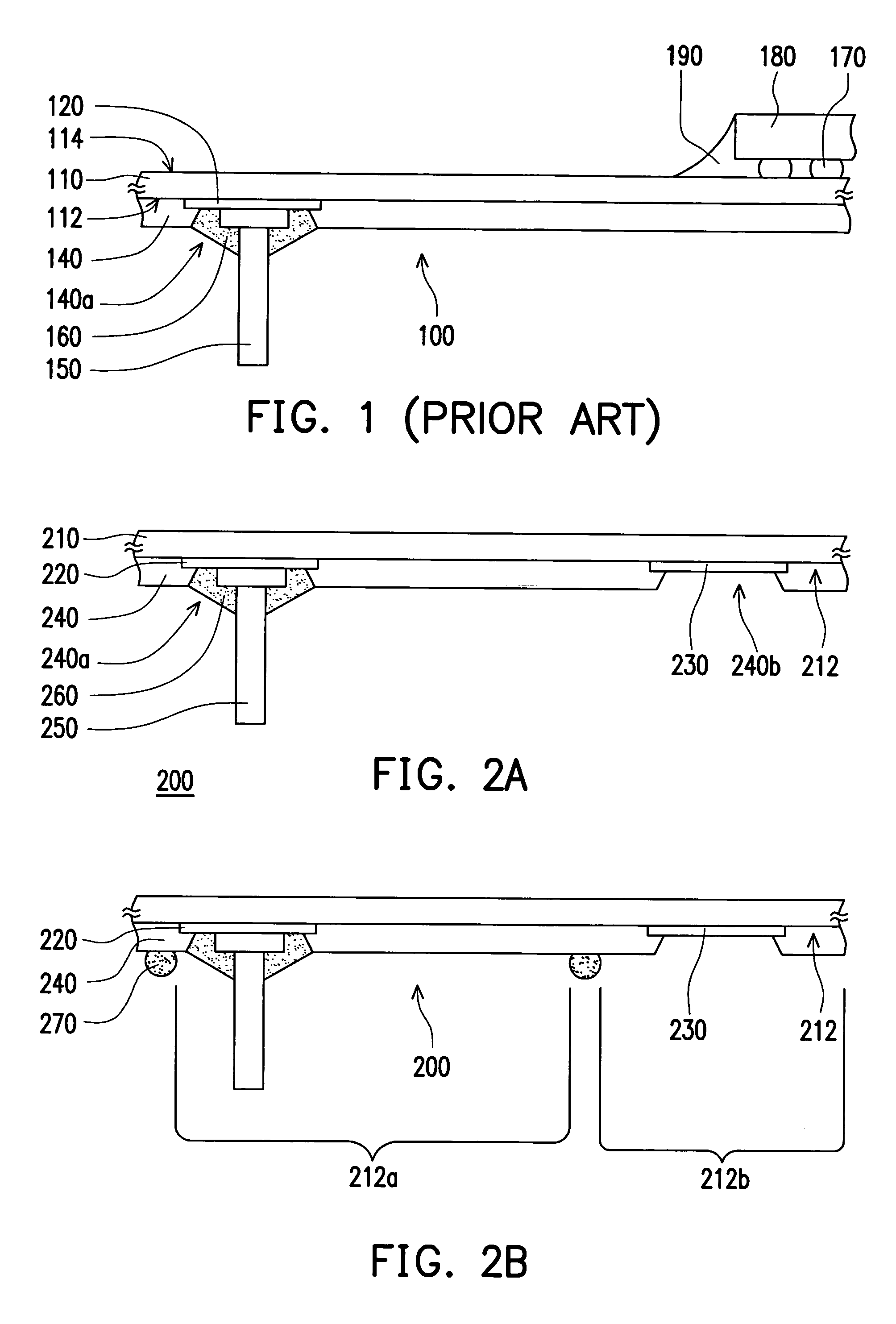
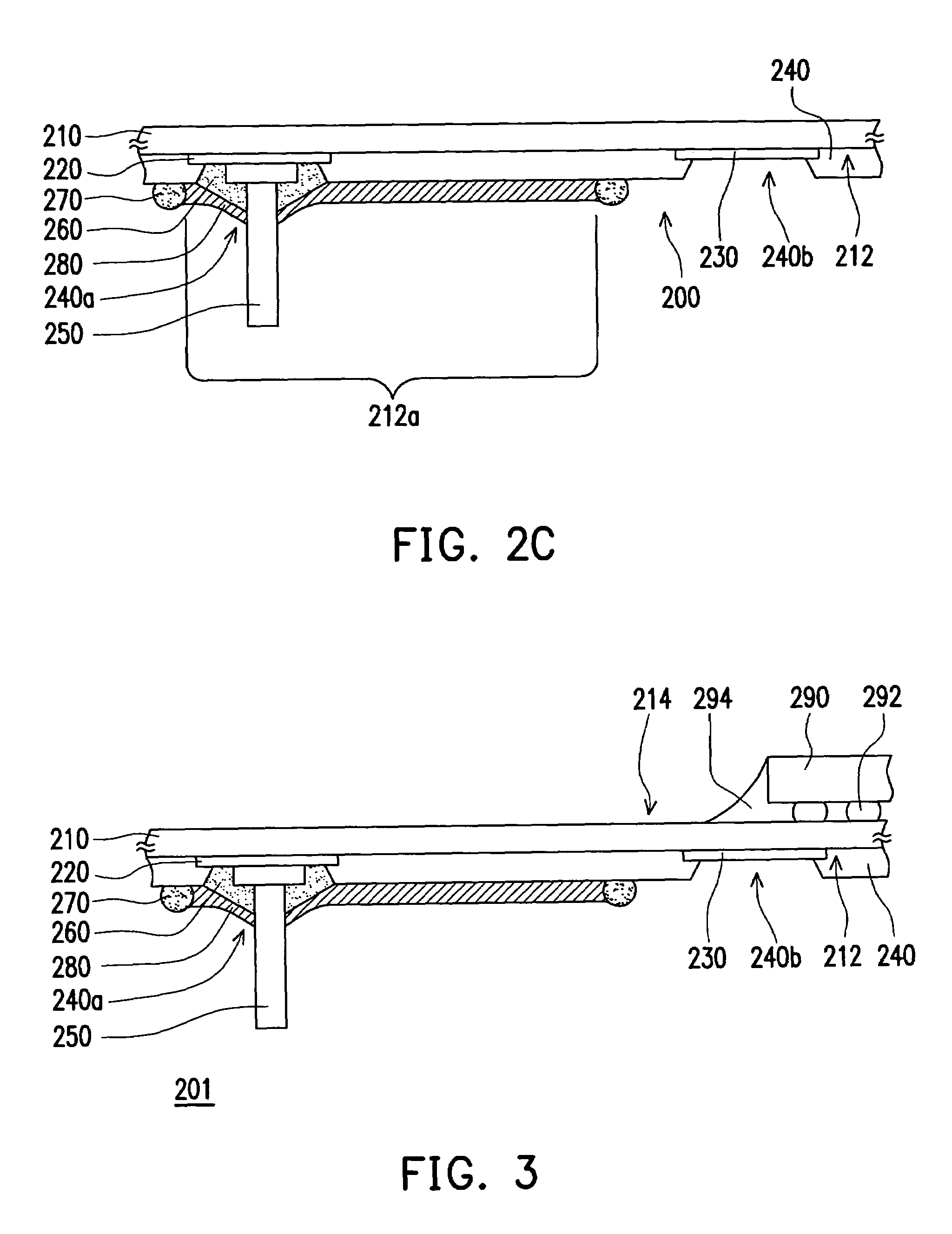
[0020]FIGS. 2A–2C is progression steps showing a fabrication method of a circuit carrier according to an embodiment of the present invention. Referring to FIG. 2A, a circuit carrier 200 is provided and adapted for a PGA package. The circuit carrier 200 comprises a substrate 210, at least one pin pad 220, at least one electrode pad 230, at least one solder mask layer 240, at least one pin 250 and at least one solder layer 260. The pin pad 220 and the electrode pad 230 are disposed over the surface 212 of the substrate 210, and may be a portion of an outer patterned circuit layer (not shown) of the substrate 210. The solder mask layer 240 is disposed over the surface 212 of the substrate 210, and comprises a plurality of solder mask openings 240a and 240b for exposing the pin pad 220 and the electrode pad 230 respectively. The solder layer 260 is disposed over the pin pad 220, and covers the pin pad 220 and a portion of a side surface of the pin 250. One end of the pin 250 connects to...


PUM


Abstract

A circuit carrier adapted for a pin grid array (PGA) package is disclosed. The circuit carrier comprises a substrate, at least one pin pad, at least one solder mask layer, at least one solder layer, at least one pin and a fixing layer. The pin pad is disposed over the surface of the substrate. The solder mask layer is disposed over the surface of the substrate, and exposing at least a portion of the pin pad. The solder layer is disposed over the pin pad. One end of the pin connects to the pin pad through the solder layer. The fixing layer is disposed over the solder mask layer, and covering the solder layer and a portion of a side surface of the pin. When the solder layer melts due to a high process temperature, the fixing layer helps to fix the pin to the pin pad.

Description

CROSS-REFERENCE TO RELATED APPLICATION[0001]This application claims the priority benefit of Taiwan application Ser. No. 93115461, filed on May 31, 2004.BACKGROUND OF THE INVENTION[0002]1. Field of the Invention[0003]The present invention relates to a circuit carrier, and more particularly to a circuit carrier adapted for a pin grid array (PGA) package.[0004]2. Description of the Related Art[0005]Due to advance of technology, a variety of electronic products have been developed. These electronic products with multiple functions are more portable and available for users, and have small sizes. Circuit carriers have been widely used in circuit layout for these electronic products. The circuit carrier can be, for example, printed circuit boards (PCB) or IC substrates. The circuit carrier is composed of a plurality of patterned circuit layers and a plurality of dielectric layers that are alternatively stacked with each other. Each dielectric layer is disposed between two patterned circuit...

Claims


Application Information

Patent Timeline
Patent Type & Authority Patents(United States)
IPC IPC(8): H01L23/48H01L21/48H01L23/498H05K3/28H05K3/34
CPCH01L21/4853H01L23/49811H05K3/3421H01L2224/16225H01L2924/15312H05K2201/10977H05K3/3452H05K2201/0195H05K2201/10318H05K3/28Y02P70/50
Inventor YANG, CHIH-AN
Owner VIA TECH INC
Why Eureka
Try Eureka