Method for implementing component placement suspended within grid array packages for enhanced electrical performance

a technology of component placement and grid array package, applied in the field of data processing, can solve the problems of reducing performance, requiring some of the most expensive circuit real-estate available, and inefficient charging, and achieve the effect of enhancing electrical performance and enhancing electrical performan

Inactive Publication Date: 2009-06-30
IBM CORP
View PDF2 Cites 5 Cited by
  • Summary
  • Abstract
  • Description
  • Claims
  • Application Information

AI Technical Summary

Benefits of technology

[0009]Principal aspects of the present invention are to provide a method and structure for implementing component placement suspended within electrical pin grid array packages for enhanced electrical performance. Other important aspects of the present invention are to provide such method and structure for implementing component placement suspended within electrical pin grid array packages for enhanced electrical performance substantially without negative effect and that overcome many of the disadvantages of prior art arrangements.
[0010]In brief, a method and structure are provided for implementing component placement suspended within electrical pin grid array packages for enhanced electrical performance. A solder column grid array is coupled between a printed circuit board and a first level package. A component is connected between a predefined pair of adjacent columns in the solder column grid array suspended between the printed circuit board and the first level package.
[0011]In accordance with features of the invention, the components are electrically connected between adjacent columns using a high temperature solder or braze. Selected components can provide column-to-column termination including power to ground connection for enhanced power decoupling. Selected components can provide column-to-column termination including one signal to another signal, for example, defining a differential pair. Selected components can provide column-to-column termination including one signal to a reference voltage plane, such as a memory termination to reference voltage Vref. The components are arranged for electrical connection within grid array packages to provide enhanced electrical performance.

Problems solved by technology

Clearly, on-chip charge is the most effective, but this also requires some of the most expensive circuit real-estate available.
A common approach is placing capacitors on the top-surface of the substrate, but due to the distance and the sometimes un-natural current path, this charge can be inefficient.
These capacitors can be effective, and they are also closer, but are still not directly in the current path and have the disadvantage of being in a longer vertical path defined by the thickness of the card, and therefore at a reduced performance.

Method used


Image

  • Method for implementing component placement suspended within grid array packages for enhanced electrical performance
  • Method for implementing component placement suspended within grid array packages for enhanced electrical performance
  • Method for implementing component placement suspended within grid array packages for enhanced electrical performance

Examples


Embodiment Construction

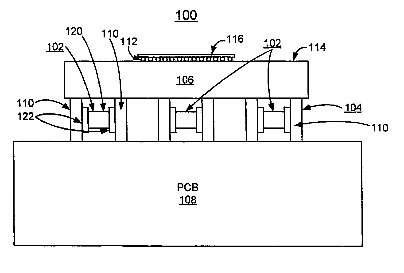
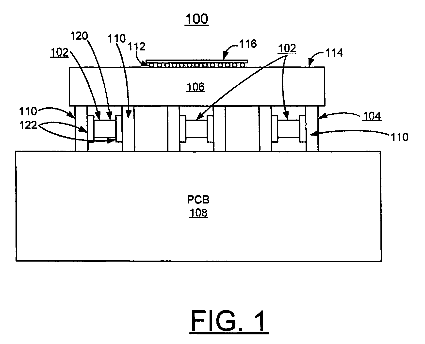
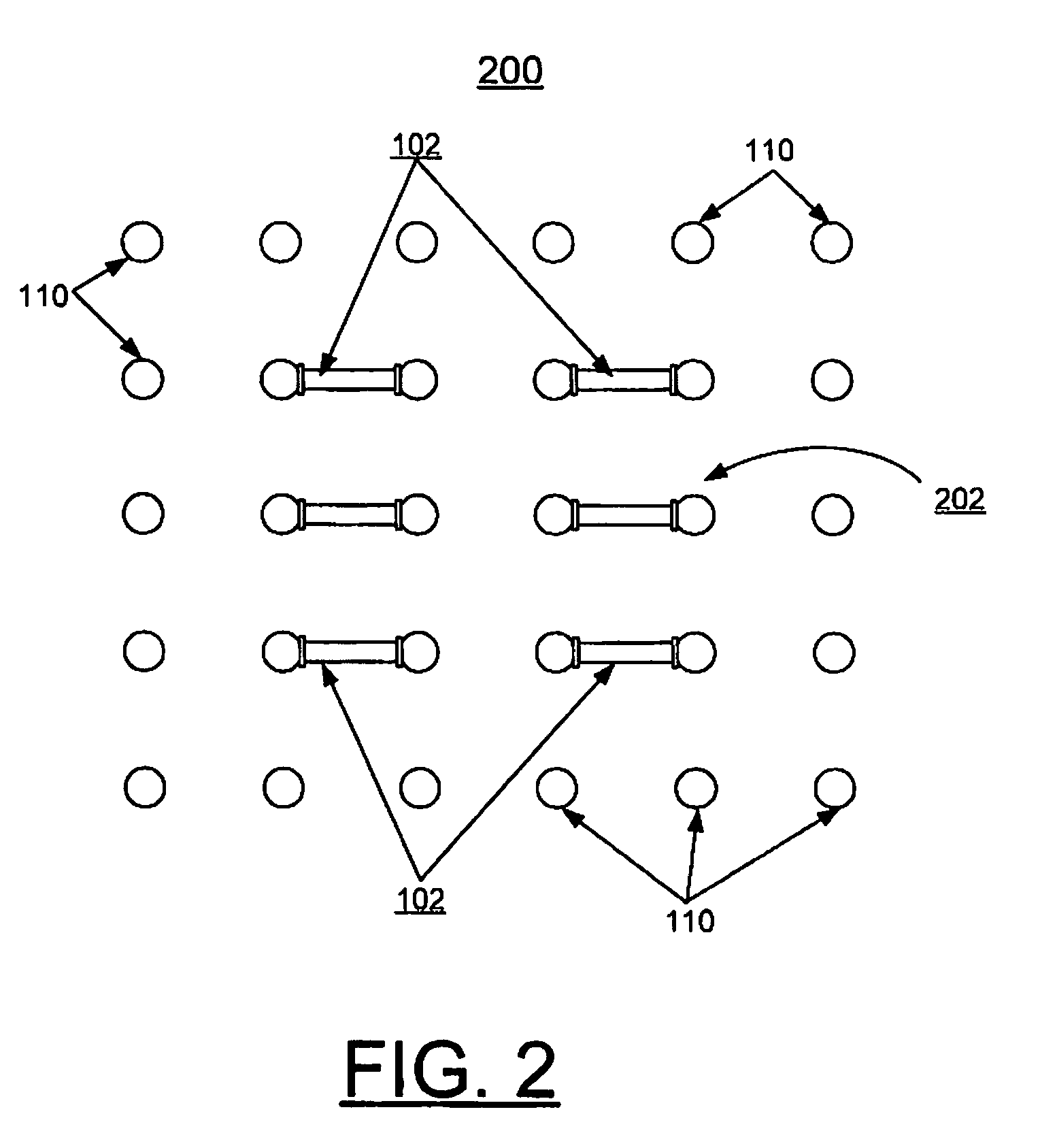
[0019]In accordance with features of the preferred embodiments, selected components are suspended within a solder column grid array that is used for first level package attach to printed circuit boards. The selected components include, for example, standard surface mount technology (SMT) capacitors, and SMT resistors. Decoupling capacitors are suspended within the solder column grid array of the electrical packaging to have a low inductive path to the noise source and can be effectively located within the current path. On-board termination requirements for resistors that are suspended within the solder column grid array of the electrical packaging, can be optimally placed nearer the receiving circuit, and with respect to on substrate filtering. By allowing the incorporation of resistors, and various small ferrite products, that are suspended within the solder column grid array, on-board termination networks are more effective and smaller than the conventional arrangements, which pla...


PUM

PropertyMeasurementUnit
poweraaaaaaaaaa
electrical performanceaaaaaaaaaa
densityaaaaaaaaaa

Abstract

A method and structure are provided for implementing component placement suspended within electrical pin grid array packages for enhanced electrical performance. A solder column grid array is coupled between a printed circuit board and a first level package. A component is connected between a predefined pair of adjacent columns in the solder column grid array suspended between the printed circuit board and the first level package.

Description

FIELD OF THE INVENTION[0001]The present invention relates generally to the data processing field, and more particularly, relates to a method and structure for implementing component placement suspended within electrical pin grid array packages for enhanced electrical performance.DESCRIPTION OF THE RELATED ART[0002]Current and future high performance computer systems and server systems rely on both large-scale packaging of multiple high density interconnect modules and printed circuit boards. High signal speed integrated circuit devices are being fabricated in increasingly smaller sizes and requiring increasing numbers of connector pins or other connection interface structures within a spatial footprint.[0003]In electronics systems there are various electronic components that require connection to other electronic components or to other levels of packaging. Examples include mounting of integrated circuit chips to a metalized substrate, multilayer ceramic substrate (MLC), laminate org...

Claims


Application Information

Patent Timeline
Patent Type & Authority Patents(United States)
IPC IPC(8): H01L21/00H01L23/48H01R43/00
CPCH05K1/0231H05K1/0246H05K3/3442H05K1/023H01L23/50Y10T29/49174H05K3/3436H05K2201/10022H05K2201/10515H05K2201/1053H05K2201/10636H05K2201/10719H05K2201/10734H05K2203/0415H01L2224/16A61K31/045A61K31/194A61K31/785H01L2924/00011H01L2924/00014Y02P70/50H01L2224/0401A61K9/0014
Inventor BARTLEY, GERALD KEITHBECKER, DARRYL JOHNDAHLEN, PAUL ERICGERMANN, PHILIP RAYMONDMAKI, ANDREW BENSONMAXSON, MARK OWEN
Owner IBM CORP
Why Eureka
Try Eureka