Wiring board and method for manufacturing the same

a wiring board and wire technology, applied in the direction of manufacturing tools, soldering devices, semiconductor/solid-state device details, etc., can solve the problems of complex manufacturing processes, large time and effort, and difficulty in reliably fitting the socket to the terminal pin, so as to facilitate easy electrical connection, facilitate easy control, and simplify the manufacturing process

Inactive Publication Date: 2012-07-26
NGK SPARK PLUG CO LTD
View PDF30 Cites 5 Cited by
  • Summary
  • Abstract
  • Description
  • Claims
  • Application Information

AI Technical Summary

Benefits of technology

[0046]Specifically, in the present embodiment, a paste-like bonding material, for instance, is placed on a terminal pad and is then heated. Solder in the bonding material is thereby fused, and an electric insulation material in the bonding material is softened. When the solder becomes subsequently solidified, terminal members can be formed. Moreover, a surface of the terminal member can be covered with the electric insulation material. Accordingly, when compared with the relate arts' manufacturing method, the present embodiment can yield a noticeable advantage in its ability to simplify the manufacturing process.
[0047]In the present embodiment, it is possible to easily control the extent to which the exposed surface of each of the terminal members is covered with solder, and, accordingly, the coverage of the exposed surface with an electric insulation material, by means of controlling the amount of bonding material used. Therefore, contr

Problems solved by technology

Thus, complicated manufacturing processes require time and effort.
For this reason, when the terminal pins is fitted into a socket, difficulty may be encountered in reliab

Method used


Image

  • Wiring board and method for manufacturing the same
  • Wiring board and method for manufacturing the same
  • Wiring board and method for manufacturing the same

Examples


first embodiment

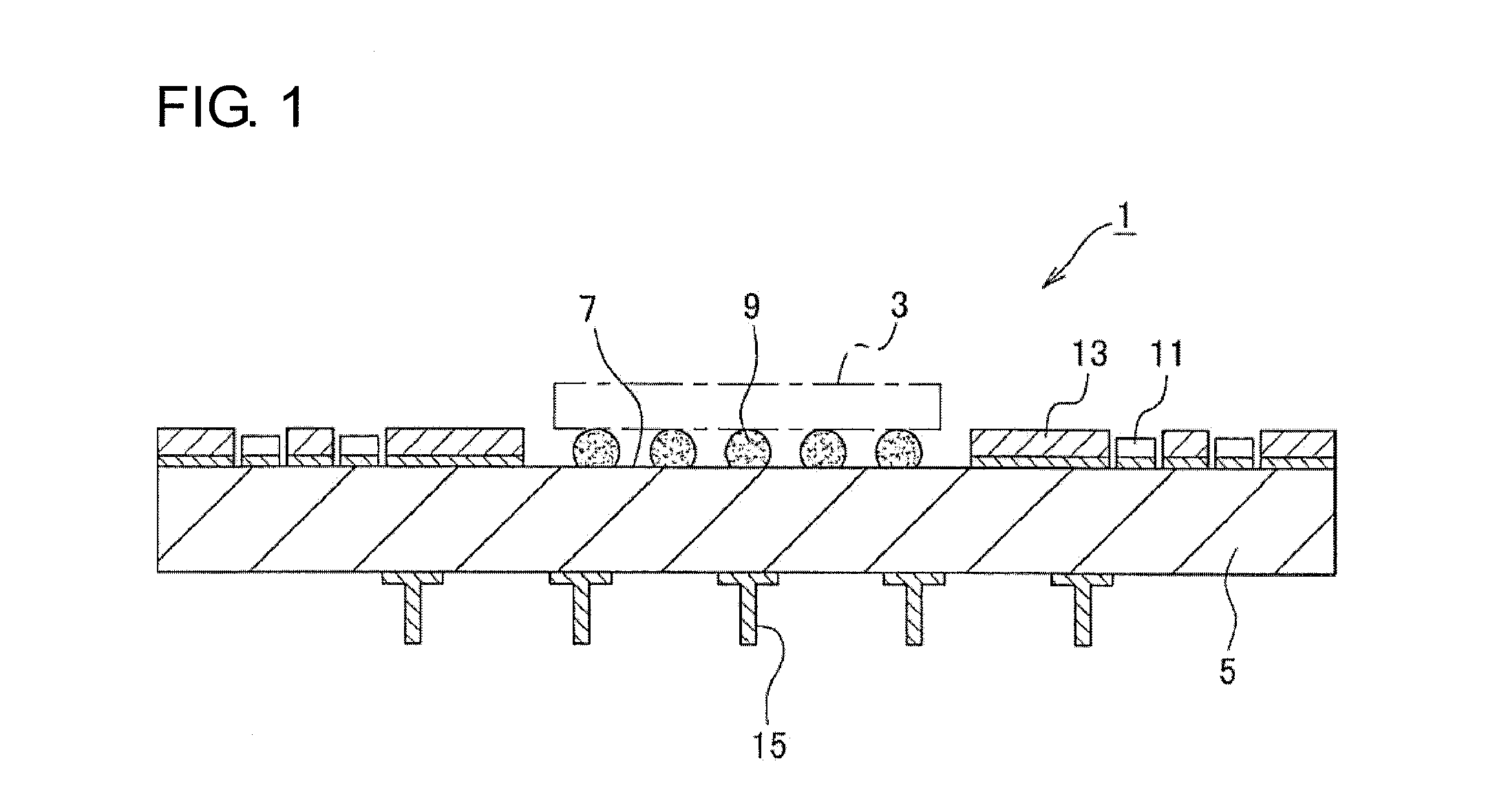
[0072]Explanations are given for, as an example, an electronic component mount wiring board (hereinafter a “wiring board”) in which an IC chip, or the like, is to be mounted on one principal surface of a coreless board.

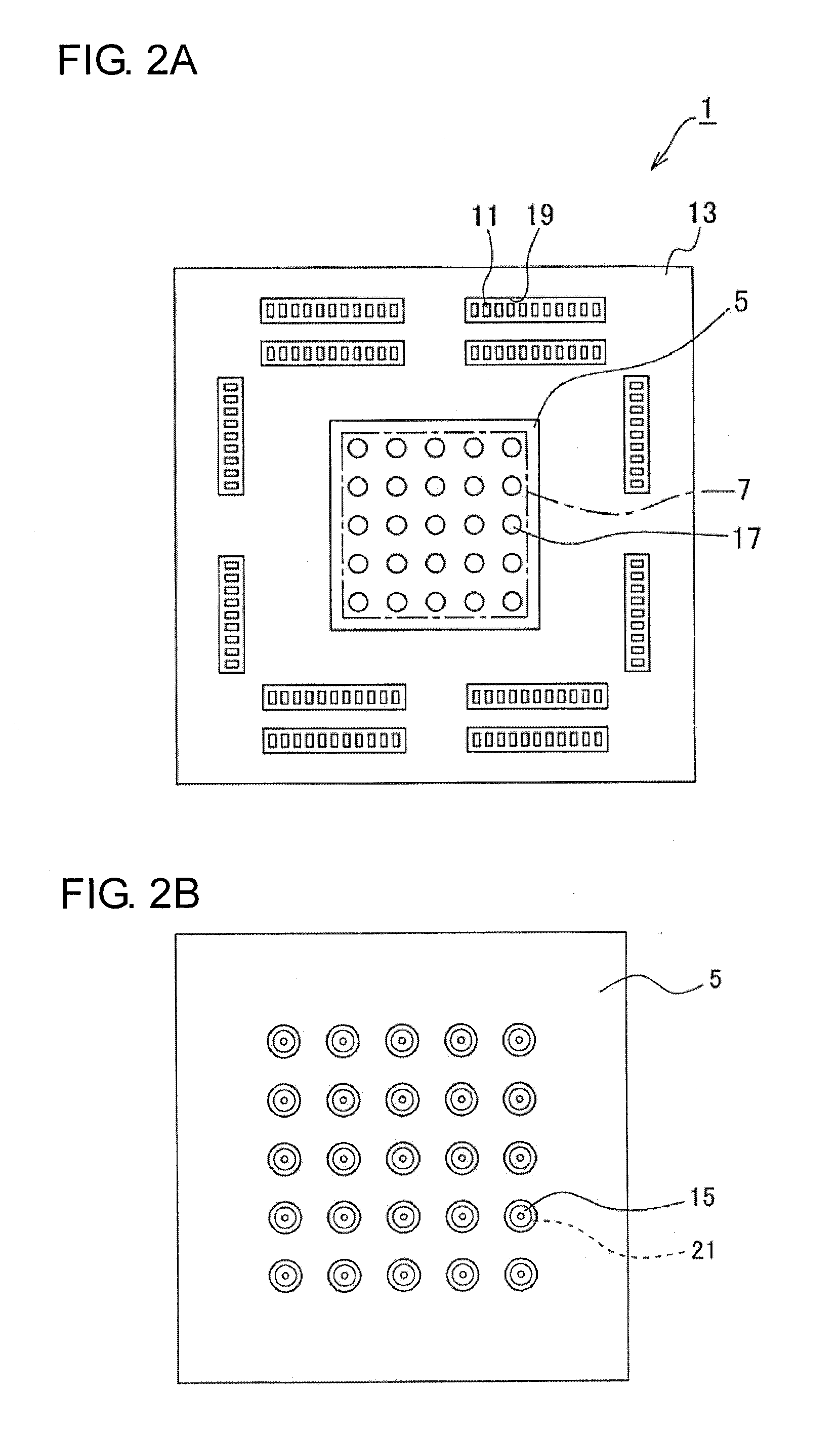
[0073]First, a configuration of a wiring board (e.g., a pin grid array) of the present embodiment is described by reference to FIGS. 1 through 4.

[0074]As shown in FIG. 1, a wiring board 1 of the present embodiment is a semiconductor package used for mounting an IC chip 3. The wiring board 1 primarily has a coreless board 5 (e.g., a multilayer board) formed so as not to include a core board.

[0075]A plurality of solder bumps 9 are formed within a mount region 7 (see FIG. 2A) of the IC chip 3 on one principal surface side (a first principal surface), which is shown as an upper side in FIG. 1 of the multilayer board 5; namely, a side of the multilayer board 5 on which the IC chip 3 is mounted. A plurality of chip capacitors 11 (CP) are mounted to a neighborhood of the mou...

second embodiment

[0133]A wiring board of a second embodiment is now described. Explanations about specific aspects that are identical with those described in connection with the first embodiment are omitted.

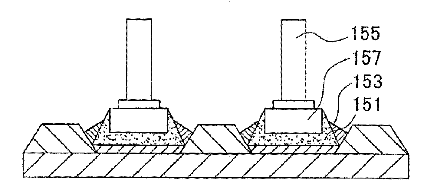
[0134]As shown in FIG. 10, a terminal pin 91 used in a wiring board 90 of the present embodiment differs in shape from its counterpart employed in the first embodiment.

[0135]Specifically, each of the terminal pins 91 used in the embodiment are made up of a base 93 and a pin 95 standing upright on the base 93. The base 93 is made up of a bottom portion 97 and an upper portion 99. In particular, the bottom portion 97 assumes a disc shape in which an entire bottom shown in a lower portion of FIG. 10 assumes a spherically convex shape.

[0136]In the embodiment, as in the first embodiment, a terminal opening 107 is formed at a position on a solder resist layer 103 formed over a surface of a multilayer board 101; namely, on a corresponding PGA terminal pad 105. The base 93 of the terminal pin 91 is bonde...

third embodiment

[0141]A wiring board and a method for manufacturing the wiring board of a third embodiment are now described. Descriptions of specific aspects that are similar to those described in connection with the first embodiment are omitted or simplified.

[0142]As shown in FIG. 11, in the wiring board (e.g., BGA board) and the method for manufacturing the wiring board of the third embodiment, the terminal member is formed not from terminal pins used in the first embodiment but from solder.

[0143]As shown in FIG. 11A, a wiring board 121 of the present embodiment has a multilayer board 123 having substantially the same structure as its counterpart described in connection with the first embodiment.

[0144]A plurality of solder bumps 127 are formed on one principal side (a first principal surface), shown as an upper side of FIG. 11A, of the multilayer board 123; namely, a side of the multilayer board 123 on which an IC chip 125 is to be mounted. A plurality of terminal members 129 are provided on the...


PUM

PropertyMeasurementUnit
Percent by massaaaaaaaaaa

Abstract

A wiring board and a method for manufacturing the wiring board reinforced by means of a resin is provided. Embodiments of the wiring board allow for reliable attachment of a connection member, like a socket, to a terminal member. For example, a base of terminal pins is put on pin grid array (PGA) terminal pads, and a bonding material paste including solder and an electric insulation material made of a resin is placed on each of the PGA terminal pads. The bonding material paste is then heated to fuse the solder and soften the electric insulation material. Subsequently, the bonding material paste is cooled to solidify the solder and bond each of the bases to a corresponding PGA terminal pad and form an electric insulation surface layer on an exposed surface of each of solder junctions to which the respective bases are bonded.

Description

CROSS REFERENCE TO RELATED APPLICATIONS[0001]The present invention claims priority from Japanese Patent Application No. 2011-011294, which was filed on Jan. 21, 2011 and Japanese Patent Application No. 2011-268119, which was filed on Dec. 7, 2011, the disclosures of which are herein incorporated by reference in its entirety.BACKGROUND OF THE INVENTION[0002]1. Field of the Invention[0003]The present invention relates to a wiring board including terminal members, like pin members, put on terminal pads of a multilayer board, such as a coreless board, made by layering conductor layers and resin insulation layers one on top of the other, as well as methods for manufacturing the same.[0004]2. Description of Related Art[0005]There has hitherto been available a semiconductor package structured in such a way that pin members (terminal pins) are attached to a wiring board as terminal members that may function as connection terminals. In such a semiconductor package, a semiconductor chip (e.g....

Claims


Application Information

Patent Timeline
IPC IPC(8): H05K1/02H05K3/46
CPCB23K1/00H01L2924/15174B23K35/22C22C11/06C22C13/00H01L24/00H05K3/4682H05K2201/10318H01L2224/81192H01L2924/15312H01L23/49811H01L23/49822H01L21/4853H01L21/6835H01L2221/68318H01L2221/68331H01L2221/68345H01L2221/68386H01L2224/16237H01L2224/814B23K35/26H01L2224/131H01L24/81H01L24/16H01L24/13H01L2924/014H01L23/12H01L23/48
Inventor INOUE, MASAHIROSAIKI, HAJIMESUGIMOTO, ATSUHIKO
Owner NGK SPARK PLUG CO LTD
Why Eureka
Try Eureka