Method and apparatus for manufacturing image display device

a technology of image display device and manufacturing method, which is applied in the manufacture of electrode systems, electric discharge tubes/lamps, instruments, etc., can solve the problems of inconvenient manufacturing method, and increased time required for the manufacturing process

Inactive Publication Date: 2004-03-09
CANON KK
View PDF8 Cites 11 Cited by
  • Summary
  • Abstract
  • Description
  • Claims
  • Application Information

AI Technical Summary

Problems solved by technology

The above-described conventional manufacturing method requires a long time for manufacturing a display panel, and is not suitable for manufacturing a display panel in which, for example, the internal pressure is 10.sup.-6 Pa or less.
Therefore, the time required for the manufacturing process is increased, thereby causing demand for significantly shortening the time of the manufacturing process.

Method used


Image

  • Method and apparatus for manufacturing image display device
  • Method and apparatus for manufacturing image display device
  • Method and apparatus for manufacturing image display device

Examples


first modified embodiment

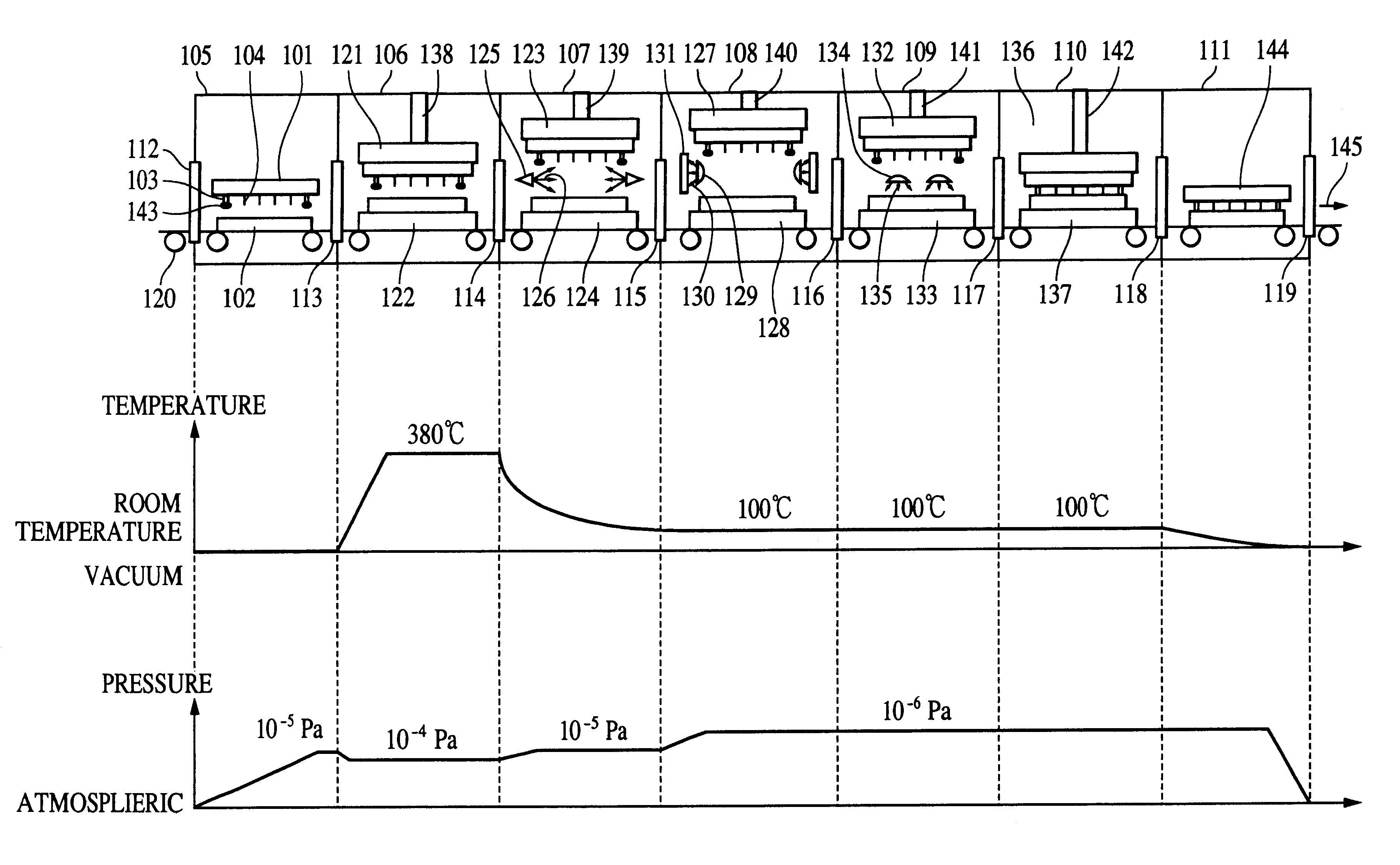
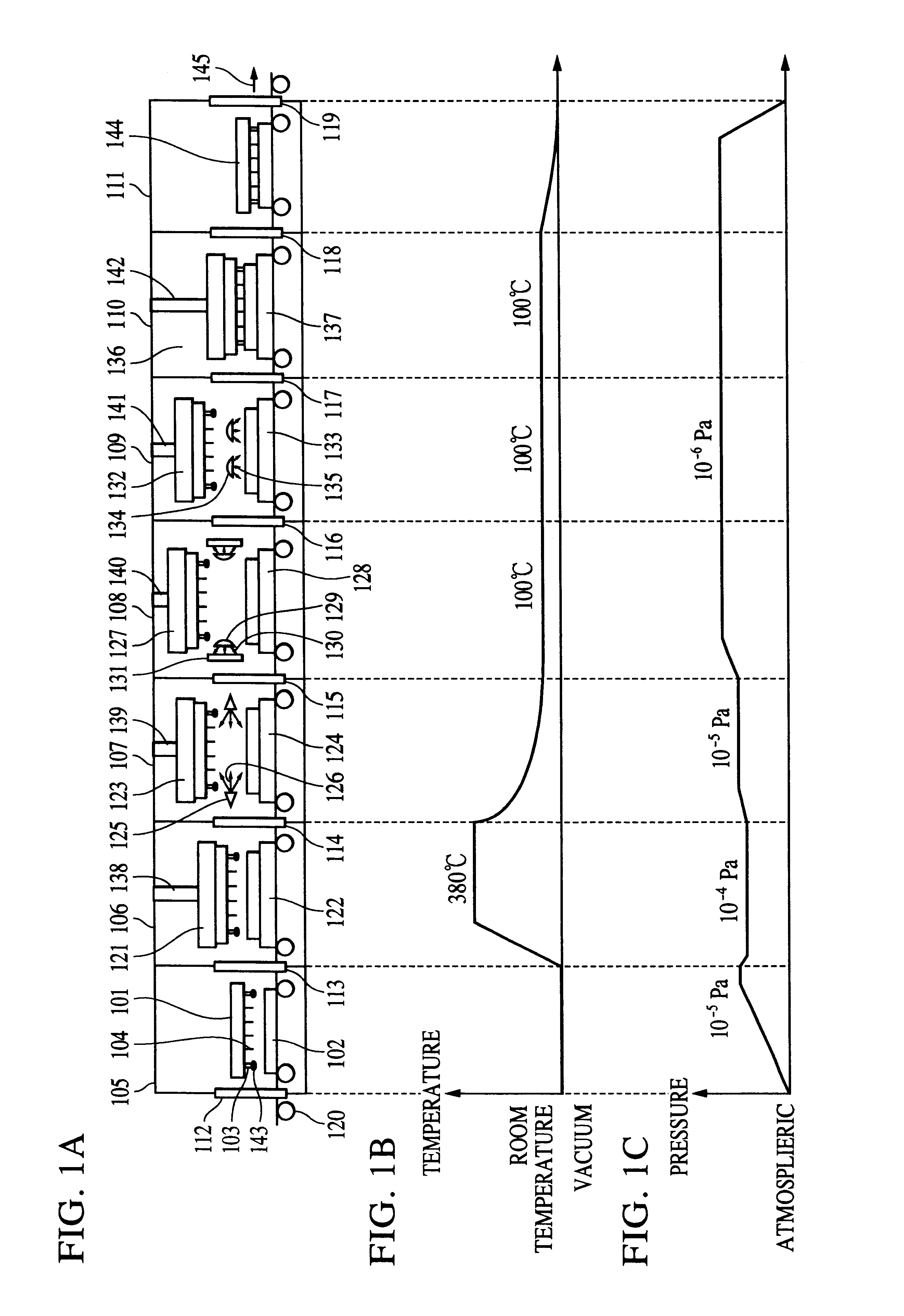
Particularly, in the process from baking to sealing, a first modified embodiment comprises the steps of preparing substrates in a vacuum atmosphere in the front chamber 105, baking in the baking chamber 106, and heat-sealing in the sealing chamber 110, which are connected in line.

second modified embodiment

A second modified embodiment comprises the steps of preparing substrates in a vacuum atmosphere in the front chamber 105, baking in the baking chamber 106, panel gettering in the panel gettering chamber 109, and heat-sealing in the sealing chamber 110, which are connected in line.

third modified embodiment

A third modified embodiment comprises the steps of preparing substrates in a vacuum atmosphere in the front chamber 105, baking in the baking chamber 106, surface cleaning by EB irradiation in the EB irradiation chamber 107, panel gettering in the panel gettering chamber 109, and heat-sealing in the sealing chamber 110, which are connected in line.


PUM

PropertyMeasurementUnit
internal pressureaaaaaaaaaa
pressureaaaaaaaaaa
pressureaaaaaaaaaa

Abstract

The present invention provides a method of manufacturing an image display device in which a panel member constituting a panel of an image display device is transferred to a plurality of processing chambers each having a temperature control unit, and subjected to a plurality of processing steps under temperature control. The temperature of the panel member in each of the processing chambers is set to be not more than the set temperature of the panel member in the previous processing chamber by the temperature control unit.

Description

1. Field of the InventionThe present invention relates to a method and apparatus for manufacturing an image display device, particularly, an image display device comprising a display panel formed by sealing a faceplate constituting the display surface of the display panel, and a rear plate arranged opposite to the faceplate with a space therebetween and constituting the back of the display panel.2. Description of the Related ArtConventional known electron emitting devices are roughly divided into two types including a thermoelectron emitting device and a cold-cathode electron emitting device. The cold-cathode electron emitting device includes field emission type (referred to as a "FE type" hereinafter), a metal / insulating layer / metal type (referred to as a "MIM type" hereinafter), and surface conduction type electron emitting devices.Known examples of the FE type are disclosed in W. P. Dyke & W. W. Dolan, "Field Emission", Advance in Electron Physics, 8, 89 (1956), C. A. Spindt, "PH...

Claims


Application Information

Patent Timeline
Patent Type & Authority Patents(United States)
IPC IPC(8): C03C23/00C03C27/06H01J9/02H01J9/26H01J9/38H01J9/39H01J9/40
CPCC03C23/0005C03C23/0075C03C27/06H01J9/38H01J9/40
Inventor NAKATA, KOHEIMIYAZAKI, TOSHIHIKOKANEKO, TETSUYA
Owner CANON KK
Why Eureka
Try Eureka