EL display using a semiconductor thin film transistor

a thin film transistor and semiconductor technology, applied in semiconductor devices, instruments, electrical equipment, etc., can solve the problems of reducing the number of possible gradations, deteriorating the frequency characteristic, and affecting the operation of external switches

Inactive Publication Date: 2004-05-04
SEMICON ENERGY LAB CO LTD
View PDF60 Cites 242 Cited by
  • Summary
  • Abstract
  • Description
  • Claims
  • Application Information

AI Technical Summary

Problems solved by technology

On the other hand, there is a tendency in that an external switch frequency characteristic is deteriorated as the current power becomes high.
As a result, there has been a problem in that as the size of the multi-gradation system EL display device is enlarged, the frequency characteristic is deteriorated, and the number of possible gradations is decreased.

Method used


Image

  • EL display using a semiconductor thin film transistor
  • EL display using a semiconductor thin film transistor
  • EL display using a semiconductor thin film transistor

Examples


embodiment 1

[Embodiment 1]

In this embodiment, there will be explained a structure of a pixel of an EL display according to the present invention.

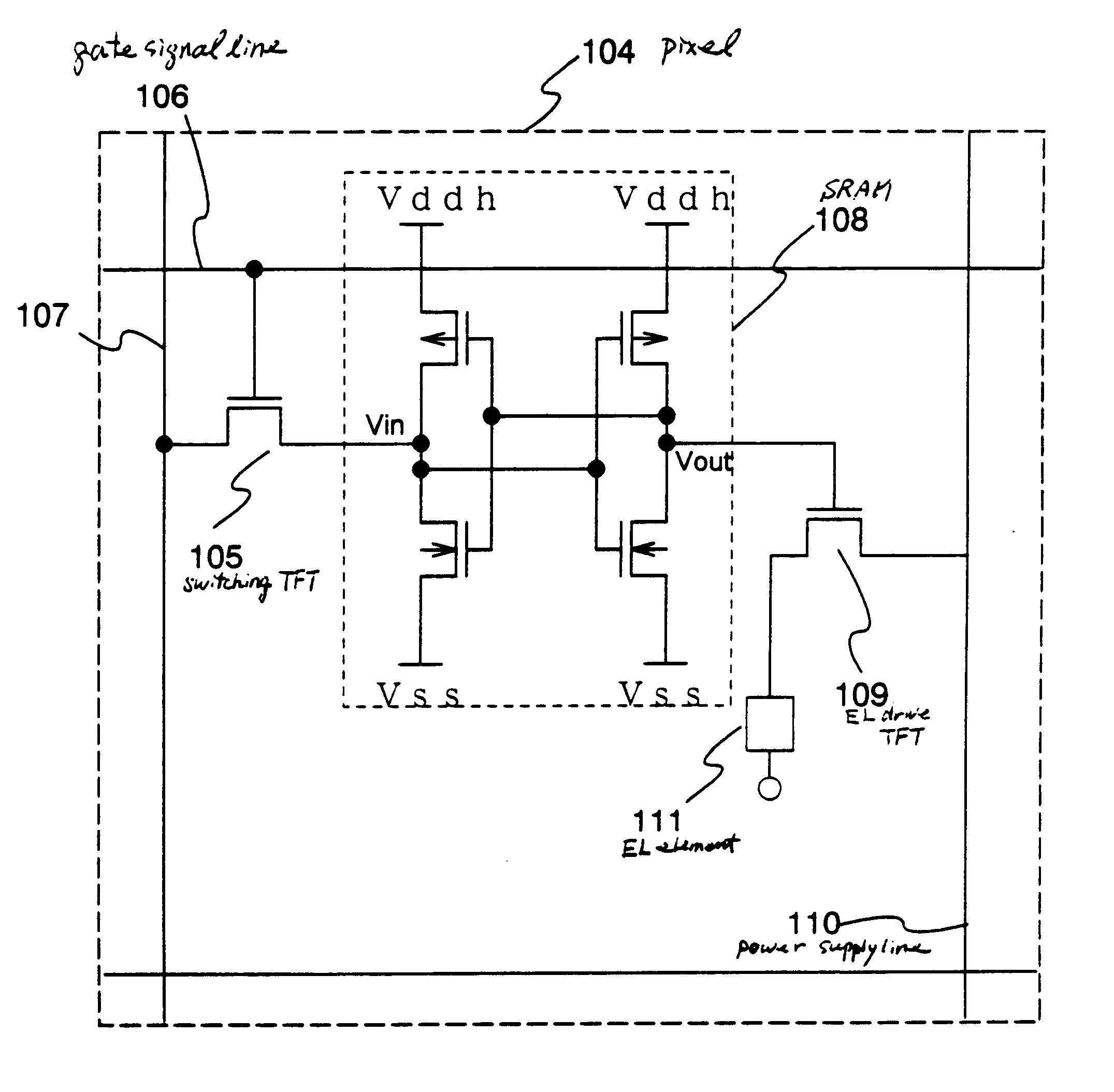
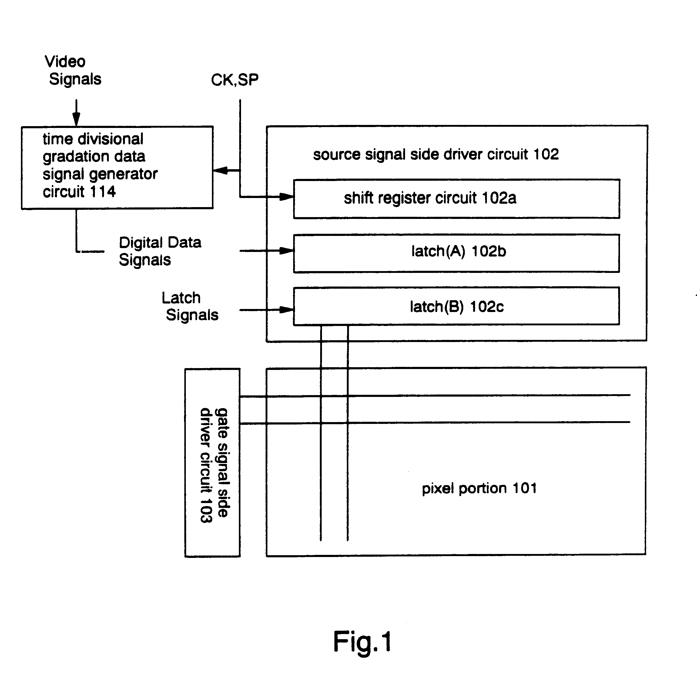
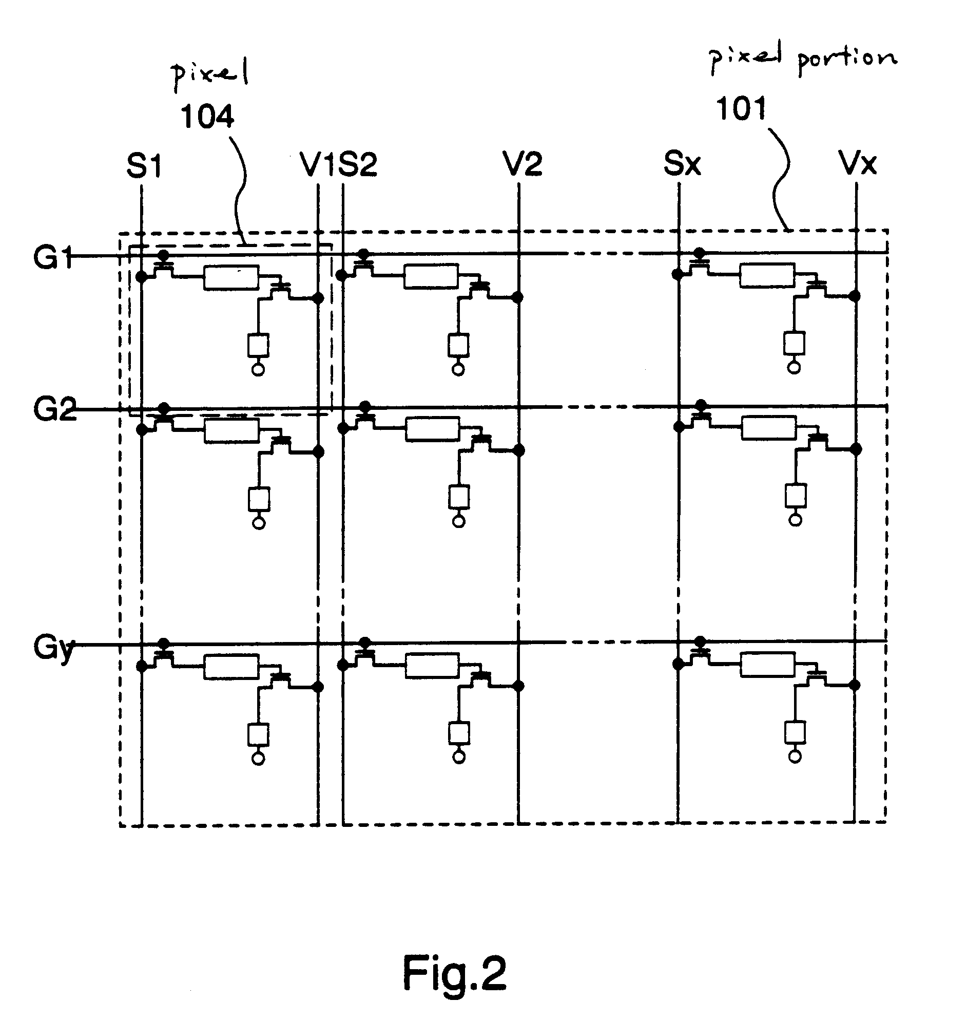
On the pixel portion of the EL display according to the present invention, a plurality of pixels is arranged in a matrix-like configuration. FIG. 7A shows an example of a circuit diagram of the pixel.

In the pixel 1000, a switching TFT 1001 is provided in FIG. 7A. Note that, in the present invention, as a switching TFT 1001, either an n-channel type TFT or a p-channel type TFT may be used. In FIG. 7A, the n-channel type TFT is used as the switching TFT 1001.

The gate electrode of the switching TFT 1001 is connected to the gate signal line 1002 for inputting a gate signal. One of the source region and the drain region of the switching TFT 1001 is connected to the source signal line (also referred to as data signal line) 1003 for inputting a digital video signal while the other is connected to the gate electrode of the EL driver TFT 1004 or capacitor 1008....

embodiment 2

[Embodiment 2]

In this embodiment, a structure of a pixel of an EL display of the present invention will be described.

In this embodiment, a power source controlling TFT is disposed between a EL driving TFT and a power source supply line. An example of a circuit diagram of a pixel is shown in FIG. 20A.

In FIG. 20A, a switching TFT 1801 is provided in a pixel 1800. In the present invention, both an n-channel TFT and a p-channel TFT may be used for the switching TFT 1801. In this embodiment, in FIG. 20A, an n-channel TFT is used for the switching TFT 1801.

A gate electrode of the switching TFT 1801 is connected to a gate signal line 1802 to which a gate signal is inputted. One of a source region and a drain region of the switching TFT 180l is connected to a source signal line (also referred to as data signal line) 1803 to which a digital video signal is inputted and the other is connected to a gate electrode of an EL driving TFT 1804 and a capacitor 1808.

One of a source region and a drain...

embodiment 3

[Embodiment 3]

An example of manufacturing an EL display using the present invention is explained in embodiment 3.

FIG. 9A is a top view of an EL display device using the present invention. In FIG. 9A, reference numeral 4010 is a substrate, reference numeral 4011 is a pixel portion, reference numeral 4012 is a source signal side driver circuit, and reference numeral 4013 is a gate signal side driver circuit. The driver circuits are connected to external equipment, through an FPC 4017, via wirings 4014 to 4016.

A covering material 6000, a sealing material (also referred to as a housing material) 7000, and an airtight sealing material (a second sealing material) 7001 are formed so as to enclose at least the pixel portion, preferably both the driver circuits and the pixel portion, at this point.

Further, FIG. 9B is a cross sectional structure of the EL display device of the present invention. A driver circuit TFT 4022 (note that a CMOS circuit in which an n-channel TFT and a p-channel TFT ...


PUM


Abstract

There is provided an electric device which can prevent a deterioration in a frequency characteristic due to a large electric power external switch connected to an opposite electrode and can prevent a decrease in the number of gradations. The electric device includes a plurality of source signal lines, a plurality of gate signal lines, a plurality of power source supply lines, a plurality of power source control lines, and a plurality of pixels. Each of the plurality of pixels includes a switching TFT, an EL driving TFT, a power source controlling TFT, and an EL element, and the power source controlling TFT controls a potential difference between a cathode and an anode of the EL element.

Description

1. Field of the InventionThe present invention relates to an EL (electro-luminescence) display formed by incorporating an EL element on a substrate. More particularly, the invention relates to an EL display (electric device) using a semiconductor element (an element using a semiconductor thin film). Furthermore, the present invention relates to an electronic apparatus (EL display device) in which the EL display is used in a display portion thereof.2. Description of the Related ArtIn recent years, technology for forming a thin film transistor (hereinafter, TFT) on a substrate has been largely improved, and an application development of the TFT to an active matrix display device has been carried out. In particular, the TFT using a polysilicon film has a higher electric field effect mobility than the TFT using a conventional amorphous silicon film, and therefore, the former TFT may be operated at a high speed. Thus, the pixel control which has been conducted at a driver circuit outside...

Claims


Application Information

Patent Timeline
Patent Type & Authority Patents(United States)
IPC IPC(8): G09G3/32G09G3/30G09G3/20H01L27/32
CPCG09G3/3275G09G3/3291H01L27/12H01L27/1214H01L27/124G09G3/2018G09G3/2022G09G2300/0417G09G2300/0426G09G2300/0809G09G2300/0842G09G2300/0861G09G2320/0233H01L27/3244H01L51/5231H01L51/5253H10K59/12H10K50/826H10K50/844G09G3/30
Inventor KOYAMA, JUN
Owner SEMICON ENERGY LAB CO LTD
Why Eureka
Try Eureka