

Capacitor and a manufacturing process therefor
a manufacturing process and capacitor technology, applied in the field of capacitors, can solve the problems of reducing the dielectric property and durability of the capacitor, applying etching technology, and difficult to form the copper electrodes in desired shap
- Summary
- Abstract
- Description
- Claims
- Application Information
AI Technical Summary
Problems solved by technology
Method used
Image

Examples
first embodiment
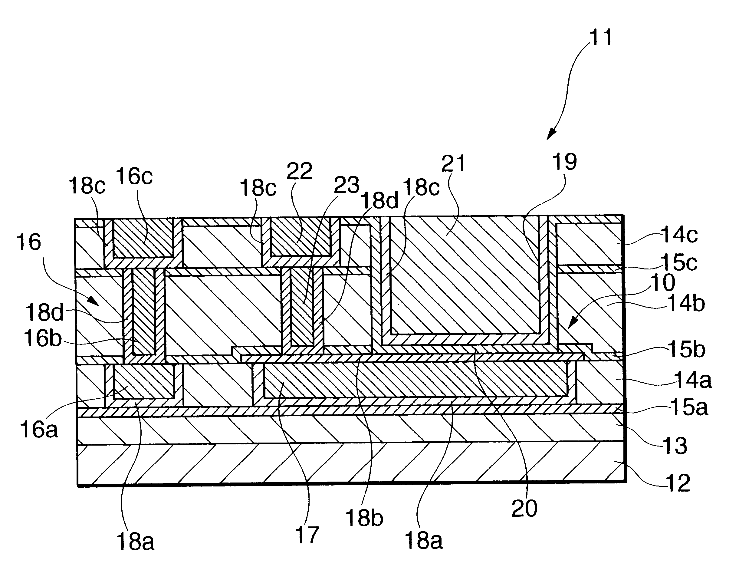
In contrast, as shown in the first embodiment, when conductive barriers 18b and 18c are used, the capacitor 10 xn be provided with a specified capacity based on the initially set thickness of the dielectric 20 regardless of variations of the barrier thickness.
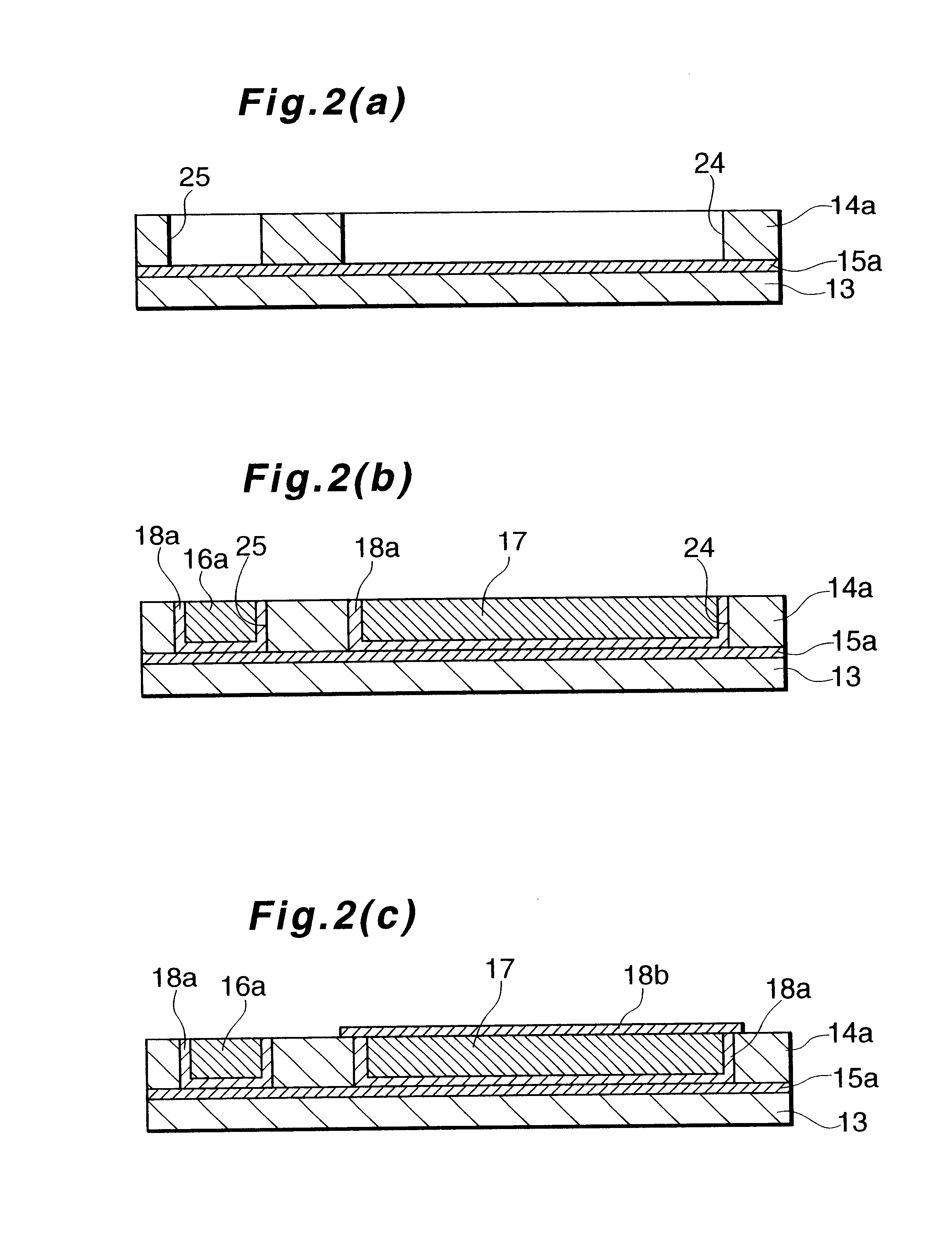
By referring to FIG. 2, description will be made of the manufacturing process of the capacitor 10 shown in FIG. 1. In FIG. 2, the semiconductor substrate 12 is omitted for simplicity of the drawing.
FIGS. 2(a) to 2(e) show the steps for forming a buried capacitor 10 by using the so-called damascene process.
As shown in FIG. 2(a), an interlayer insulating film 13 is formed on the semiconductor substrate 12 (not shown), and a SiN film 15a to serve as an etching stopper film is formed on the interlayer insulating film. Though this is not shown, a through-hole leading to the circuit portion under the interlayer insulating film 13 is formed, when necessary, in the SiN film 15a and the interlayer insulating film 13.
Thereafter, a lower ...
second embodiment
FIG. 2 resembles the drawing in FIG. 1, but shows the capacitor according to the present invention.
In the capacitor in the second embodiment, an upper electrode 30 made of tungsten is used instead of the upper electrode 21 in the first embodiment. As the dielectric, a SiN film 15c is used, which serves as an etching stopper.
A recess 19 for the upper electrode 30 is formed in the intermediate layer of the interlayer insulating film 14. The SiN film 15c, which covers the upper surface of the intermediate insulating layer 14b, extends to cover the wall of the recess 19.
The upper tungsten electrode 30 is accommodated in the recess 19 covered with the SiN film 15c with interposition of the nitrided metal layer 18d, which has conductivity as mentioned above.
The upper electrode 30 forms a capacitor 10 in cooperation with the lower electrode 17 and the SiN film, which is a dielectric film and located between the upper electrode 30 and the lower electrode 17.
third embodiment
In the capacitor 10 in the third embodiment, which has the upper electrode 33 made of a conductive nitrided metal layer, such as a TiN film, to reduce the high resistance of the upper electrode 33, the area of the wiring pattern 31 should preferably be made equal to or larger than that of the upper electrode 33.
According to the method shown in FIG. 4, as in the second embodiment, because the barrier that prevents the deterioration of the insulating films caused by copper metal can be utilized as the seed layer in copper plating, an integrated circuit 11 excellent in high-frequency characteristics and having the wiring pattern 31 provided on the upper electrode can be formed efficiently without incurring the deterioration of the insulating film ascribable to the diffusion of copper atoms.
Further, in the first and second embodiments, the dielectric 15c or 20 has its peripheral portion rising along the outer periphery of the upper electrode 21 or 30. In the third embodiment, on the oth...
PUM
| Property | Measurement | Unit |
|---|---|---|
| dielectric | aaaaa | aaaaa |
| conductive | aaaaa | aaaaa |
| non-conducting | aaaaa | aaaaa |
Abstract
Description
Claims
Application Information