

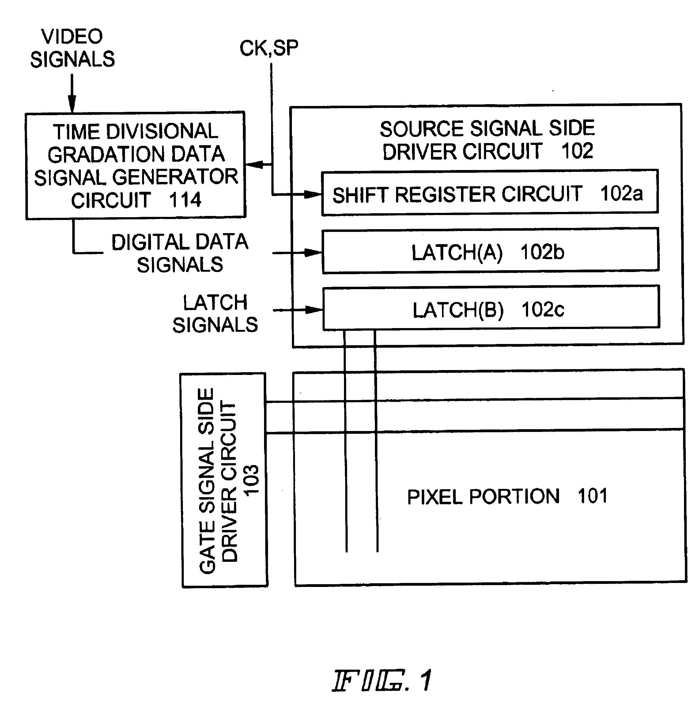
Active matrix display with pixel memory
a technology of active matrix and pixel memory, applied in the field of el (electroluminescence) display, can solve the problems of not achieving desired gradation, reducing the brightness of light emitted by the el element, and gradually reducing the electric charg
- Summary
- Abstract
- Description
- Claims
- Application Information
AI Technical Summary
Benefits of technology
Problems solved by technology
Method used
Image

Examples
embodiment 1
[Embodiment 1]
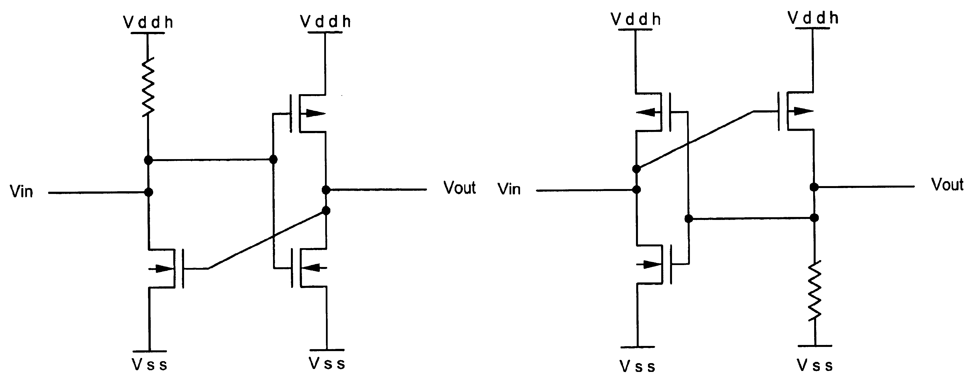
An SRAM structure used by the present invention, differing from that shown by FIG. 4, is explained in embodiment 1.
An equivalent circuit diagram of the SRAM of embodiment 1 is shown in FIG. 6. The SRAM has two n-channel TFTs and two resistors. One n-channel TFT and one resister form a pair, and two n-channel TFT and resistor pairs exist within one SRAM. A drain region of the n-channel TFT is connected to a high voltage side electric power supply Vddh, and a source region of the n-channel TFT is connected, through the resistor, to a low voltage side electric power supply Vss.
The drain region of the n-channel TFT is maintained at the same electric potential as a gate electrode of the other n-channel TFT. One n-channel TFT drain region is an input side for inputting an input signal Vin, and the other n-channel TFT drain region is an output side for outputting an output signal Vout.
The SRAM is designed so as to store Vin, and to output Vout, a signal in which Vin is invert...
embodiment 2
[Embodiment 2]
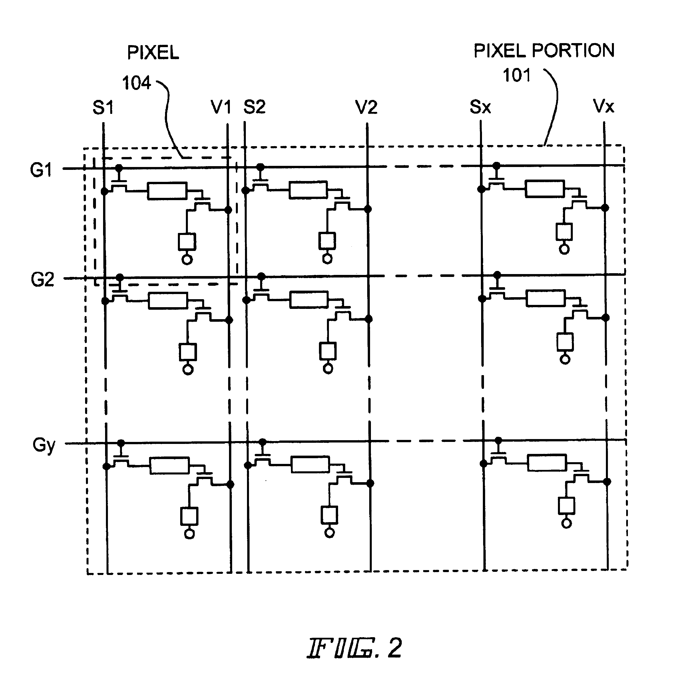
In Embodiment 2, there will be explained a structure of a pixel of an EL display according to the present invention.
On the pixel portion of the EL display according to the present invention, a plurality of pixels is arranged in a matrix-like configuration. FIG. 7A shows an example of a circuit diagram of the pixel.
In the pixel 1000, a switching TFT 1001 is provided in FIG. 7A. Note that, in the present invention, as a switching TFT 1001, either an n-channel type TFT or a p-channel type TFT may be used. In FIG. 7A, the n-channel type TFT is used as the switching TFT 1001.
The gate electrode of the switching TFT 1001 is connected to the gate signal line 1002 for inputting a gate signal. One of the source region and the drain region of the switching TFT 1001 is connected to the source signal line (also referred to as data signal line) 1003 for inputting a digital data signal while the other is connected to the input side of the SRAM 1008. The output side of a SRAM 1008 is ...
embodiment 3
[Embodiment 3]
An example of manufacturing an EL display using the present invention is explained in embodiment 3.
FIG. 9A is a top view of an EL display device using the present invention. In FIG. 9A, reference numeral 4010 is a substrate, reference numeral 4011 is a pixel portion, reference numeral 4012 is a source signal side driver circuit, and reference numeral 4013 is a gate signal side driver circuit. The driver circuits are connected to external equipment, through an FPC 4017, via wirings 4014 to 4016.
A covering material 6000, a sealing material (also referred to as a housing material) 7000, and an airtight sealing material (a second sealing material) 7001 are formed so as to enclose at least the pixel portion, preferably the driver circuits and the pixel portion, at this point.
Further, FIG. 9B is a cross sectional structure of the EL display device of the present invention. A driver circuit TFT 4022 (note that a CMOS circuit in which an n-channel TFT and a p-channel TFT are c...
PUM
 Abstract
Description
Claims
Application Information