Light emitting device, electronic equipment, and method of manufacturing thereof

a technology of light emitting devices and electronic equipment, which is applied in the direction of discharge tubes/lamp details, discharge tubes luminescnet screens, electric discharge lamps, etc., can solve the problems of degrading the device by heat, light, moisture, and oxygen easily reaching

Inactive Publication Date: 2004-11-23
SEMICON ENERGY LAB CO LTD
View PDF31 Cites 57 Cited by
  • Summary
  • Abstract
  • Description
  • Claims
  • Application Information

AI Technical Summary

Benefits of technology

When manufacturing a light-emitting device with OLED, in general, the OLED is formed after a wiring line and a semiconductor element are formed in a pixel portion. Once the OLED is formed, a first substrate on which the OLED is placed is bonded to a second substrate (made of metal or glass) for sealing (packaging) the OLED so that the OLED is not exposed to the outside air. A resin or the like is used to bond the substrates and nitrogen or inert gas fills the space between the substrates. However, oxygen easily reaches the OLED sealed as above by the substrates and a resin through the slightest crack in the package. Furthermore, moisture finds no difficulty in seeping into the OLED through the resin used in bonding and sealing. This causes non-light emission portions called dark spots, which grow larger with time and emit no light, which becomes a problem.
In the present invention, a film low in gas transmissivity is used to provide a film while adding a rare gas element to reaction gas in order to give the film flexibility. The present invention is characterized in that a thin film low in gas transmissivity (typically, a thin film mainly containing carbon, a silicon oxynitride film, a silicon nitride film, a film of a compound expressed as AlN.sub.X O.sub.Y, a AlN film, or a laminate of these films) contains a rare gas element to ease the internal stress in the film and to make the film flexible, and that a film provided, at least on one side (inside), with the thin film is used to vacuum-seal a light-emitting device having an OLED.
A film obtains flexibility by containing rare gas. Therefore, the thin film used to provide the wrapping film is prevented from developing a crack or peeling off when thermally press-fit in vacuum. Moreover, the film used as a lining can improve the heat resistance and mechanical strength of the wrapping film.
A DLC film is formed by plasma CVD, microwave CVD, electron cyclotron resonance (ECR) CVD, sputtering, etc. Any of these methods can provide a DLC film having an appropriate adhesion. A DLC film is formed by setting a substrate as the cathode. When a negative bias is applied and some of ion impact is utilized, a dense and hard DLC film can be obtained.
Reaction gas used in forming a DLC film by plasma CVD is hydrocarbon-based gas, for example, CH.sub.4, C.sub.2 H.sub.2, or C.sub.6 H.sub.6. The reaction gas is ionized by glow discharge and the ions are accelerated to impact against a cathode to which a negative self-bias is applied. As a result, a dense and flat DLC film can be obtained.

Problems solved by technology

The problem in putting a light-emitting device using the OLED into practice is degradation of the device by heat, light, moisture, oxygen, and other causes.
However, oxygen easily reaches the OLED sealed as above by the substrates and a resin through the slightest crack in the package.
This causes non-light emission portions called dark spots, which grow larger with time and emit no light, which becomes a problem.

Method used


Image

  • Light emitting device, electronic equipment, and method of manufacturing thereof
  • Light emitting device, electronic equipment, and method of manufacturing thereof
  • Light emitting device, electronic equipment, and method of manufacturing thereof

Examples


embodiment mode 1

[Embodiment Mode 1]

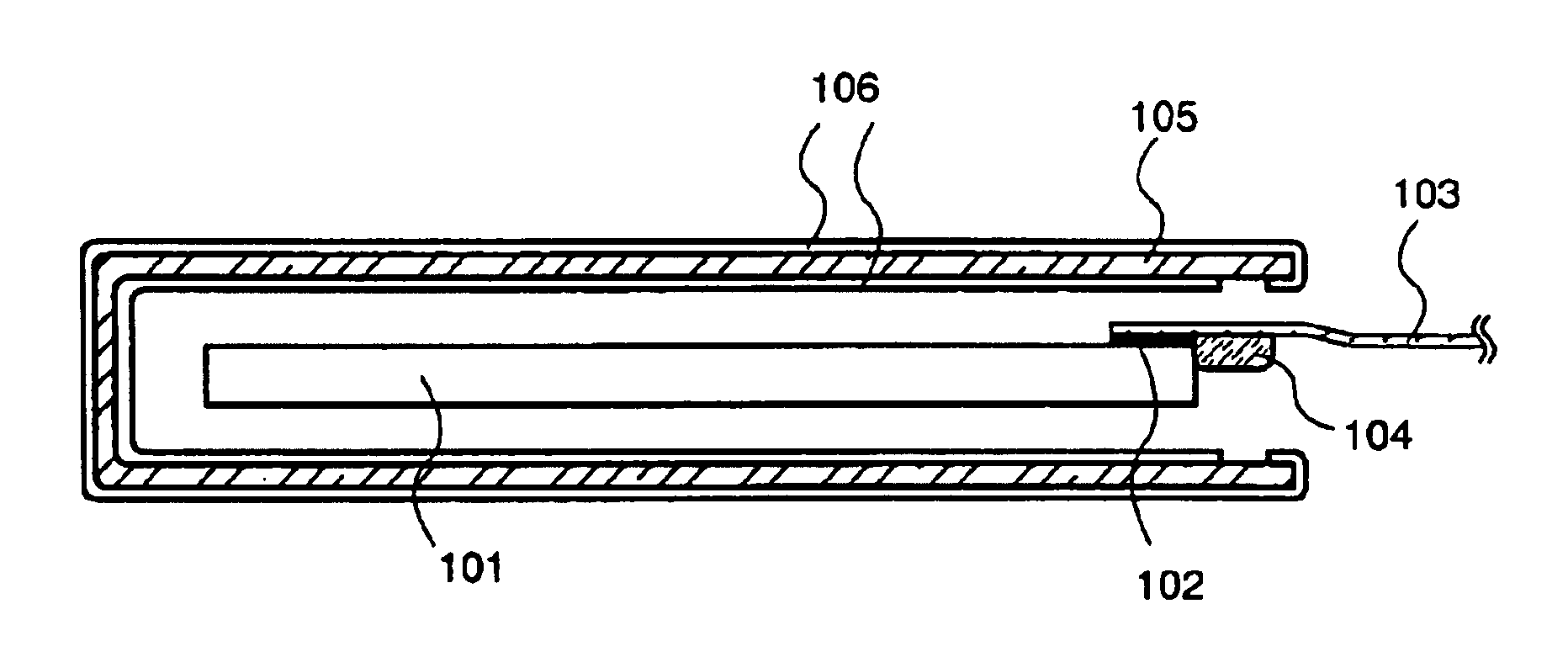
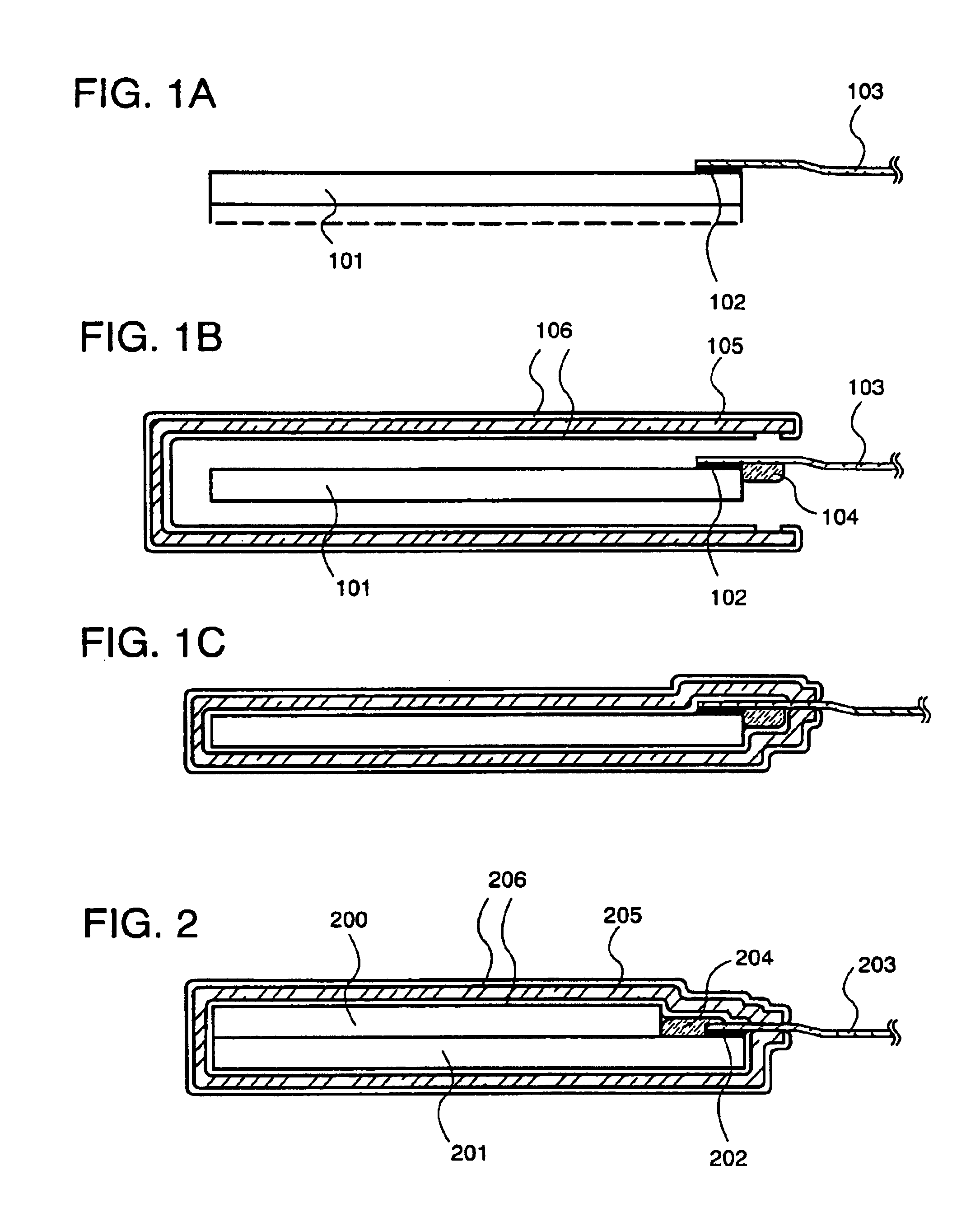
First, a substrate having an insulating surface is prepared. On the substrate, a light emitting element, here, OLED, and a lead-out electrode 102 are provided. The lead-out electrode 102 connects the OLED to an external power supply. If light from the light emitting element is transmitted through the substrate, used as the substrate having an insulating surface is a light transmissive substrate such as a glass substrate, a crystallized glass substrate, or a plastic substrate. If light from the light emitting element does not travel through the substrate, a ceramic substrate, a semiconductor substrate, a metal substrate, and the like may be used.

In order to reduce the weight of the device, etch off treatment is performed on the substrate and the substrate is thinned. A substrate 101 having the OLED formed thereon is thus obtained. The etch off treatment may not always be necessary. Next, a flexible printed substrate (FPC) 103 is bonded to the substrate 101 to be el...

embodiment mode 2

[Embodiment Mode 2]

A description given here with reference to FIG. 2 is about an example of a light-emitting device in which an OLED is sealed using a sealing substrate 200 and then further sealed by a protective unit.

In FIG. 2, 200 denotes a sealing substrate, 201, a substrate having an OLED formed thereon, 202, a lead-out electrode, 203, an FPC, 204, a desiccant, 205, a wrapping film, and 206, a DLC film containing Ar. Although the film 206 here is a DLC film containing Ar, the DLC film may be replaced by a silicon oxynitride film containing Ar, a silicon nitride film containing Ar, a Ar-containing film of a compound expressed as AlN.sub.X O.sub.Y, or a AlN film containing Ar.

By containing Ar, the film can be flexible and therefore can be prevented from developing a crack or peeling off when used to provide the wrapping film and thermally press-fit in vacuum.

Though not shown in the drawing, the sealing substrate 200 is bonded to the substrate 201 with an adhesive. The space betwee...

embodiment 1

[Embodiment 1]

FIG. 4A is a top view of an OLED module manufactured. FIG. 4B is a sectional view schematically showing one pixel of the module of FIG. 4A.

A pixel portion 404 is arranged on a substrate 401 such that a source line driving circuit 402 and a gate line driving circuit 403 respectively run parallel to two sides of the pixel portion. The pixel portion 404, the source line driving circuit 402, and the gate line driving circuit 403 each have a plurality of TFTs. FIG. 4B shows, as representatives of those TFTs, a driving circuit TFT (composed of an n-channel TFT and a p-channel TFT in FIG. 4B) 411 included in the source line driving circuit 402 and a driving TFT (a TFT for controlling a current flowing into the OLED) 412 included in the pixel portion 404. The TFTs 411 and 412 are formed on a base film 410.

In this embodiment, the n-channel TFT and the p-channel TFT that constitute the driving circuit TFT 411 are manufactured by a known method, and a p-channel TFT manufactured b...


PUM


Abstract

A highly reliable light-emitting device is provided in which an organic light-emitting device is not degraded by oxygen, moisture, and the like. The organic light-emitting device is press-fit in vacuum using a wrapping film (105) that is covered with a DLC film (or a silicon nitride film, an AlN film, a film of a compound expressed as AlNXOY) (106) containing Ar. The organic light-emitting device thus can be completely shut off from the outside, and moisture, oxygen, or other external substances that accelerate degradation of an organic light emitting layer can be prevented from entering the organic light-emitting device.

Description

1. Field of the InventionThe present invention relates to an OLED (organic light-emitting device) panel obtained by forming an OLED on a substrate and sealing the OLED between the substrate and a cover member. The invention also relates to an OLED module in which an IC including a controller, or the like, is mounted to the OLED panel. In this specification, `light-emitting device` is the generic term for the OLED panel and for the OLED module. Electronic equipment using the light-emitting device is also included in the present invention.2. Description of the Related ArtBeing self-luminous, OLEDs eliminate the need for a backlight that is necessary in liquid crystal display devices (LCDs) and thus make it easy to manufacture thinner devices. Also, the self-luminous OLEDs are high in visibility and have no limit in terms of viewing angle. These are the reasons for attention that light-emitting devices using the OLEDs are receiving in recent years as display devices to replace CRTs and...

Claims


Application Information

Patent Timeline
Patent Type & Authority Patents(United States)
IPC IPC(8): H01L51/50H01L51/52H01L27/32H01L27/28
CPCH01L51/5237H01L27/3244H10K59/12H10K50/841H10K50/846H10K50/844
Inventor YAMAZAKI, SHUNPEIMARUYAMA, JUNYAOGURA, KEIICHITAKAYAMA, TORU
Owner SEMICON ENERGY LAB CO LTD
Why Eureka
Try Eureka