Full color organic EL display panel, manufacturing method thereof and driving circuit thereof

a technology of organic el and display panels, applied in the direction of discharge tubes luminescnet screens, instruments, static indicating devices, etc., can solve the problems of increasing connection capacitance, line resistance can be a more serious obstacle, and the connection capacitance can be increased, so as to improve luminance efficiency and improve luminance efficiency. , the effect of poor luminance efficiency of red pixels

Inactive Publication Date: 2005-01-04
LG ELECTRONICS INC
View PDF4 Cites 23 Cited by
  • Summary
  • Abstract
  • Description
  • Claims
  • Application Information

AI Technical Summary

Benefits of technology

According to the invention, the light emitting pixels are composed into an array structure in which red, green and blue pixels have different areas ac

Problems solved by technology

However, the major problem of the organic EL device is the connection capacitance, which includes the capacitance within the device composed of the material and the electrode and the capacitance from column and line electrodes in an array structure.
Further, the transparent electrode layer is made of a high resistive material thereby increasing such a problem.
Therefore, the connection capacitance and the electrode layer having high resistance of the organic EL device hinder producing the EL device in a large array structure.
However, in a delta shaped array structure, such line resistance can be a more serious obstacle due to the fine cathode line.
In particular, in the case of the A material (for the R pixels for example) which is poor in the current-voltage features, a higher current is required to obtain the white

Method used


Image

  • Full color organic EL display panel, manufacturing method thereof and driving circuit thereof
  • Full color organic EL display panel, manufacturing method thereof and driving circuit thereof
  • Full color organic EL display panel, manufacturing method thereof and driving circuit thereof

Examples


first embodiment

FIG. 3A to FIG. 3K are plan views for showing a process of manufacturing a full color EL display device according to the first embodiment of the invention.

As shown in FIG. 3A, a pattern of anode lines 102-2 is formed on a glass 101 by using ITO or other transparent electrodes. Here, light emitting pixels 102-1 are formed into the shape of a polygon with at least three angles, and have the area for emitting a red light larger than that for emitting blue and green lights. Half of the area of the light emitting pixels 102-1 is arranged for red, and the other area is arranged for blue and green. Another pattern of anode lines is also formed under light emitting pixels 102-1.

Then, as shown in FIG. 3B, auxiliary electrodes 105 are formed in anode lines 102-2 which connect the light emitting pixels 102-1, in order to reduce the resistance of the anode lines 102-2. When the auxiliary electrodes 104 are provided around the light emitting pixels 102-1 also, the resistance can be further reduc...

second embodiment

FIG. 8A to FIG. 8L are a plan view for showing a process for manufacturing a full color organic EL display device according to the second embodiment of the invention.

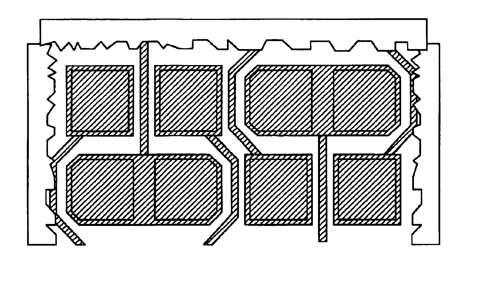
First, as shown in FIG. 8A, patterns of anode lines 202-1 and 202-2 are formed on a glass 201 with ITO or other transparent electrodes. The anode lines 202-1 and 202-2 are patterned into the above shape so that each unit of light emitting pixels 202-3 is divided along diagonal directions into four sub-pixels 202-4 shaped as a triangle with smooth comers. The unit light emitting pixel 202-3 comprised of the sub-pixels 202-4 is provided with light emitting material layers for emitting red, green and blue lights.

In the sub-pixels 202-4 structured as above, a pair of sub-pixels opposed in the diagonal direction applied with red light emitting material layers which will emit low red lights with relatively low luminous efficiency, and another pair of sub-pixels are applied with blue and green light emitting material layers to...

third embodiment

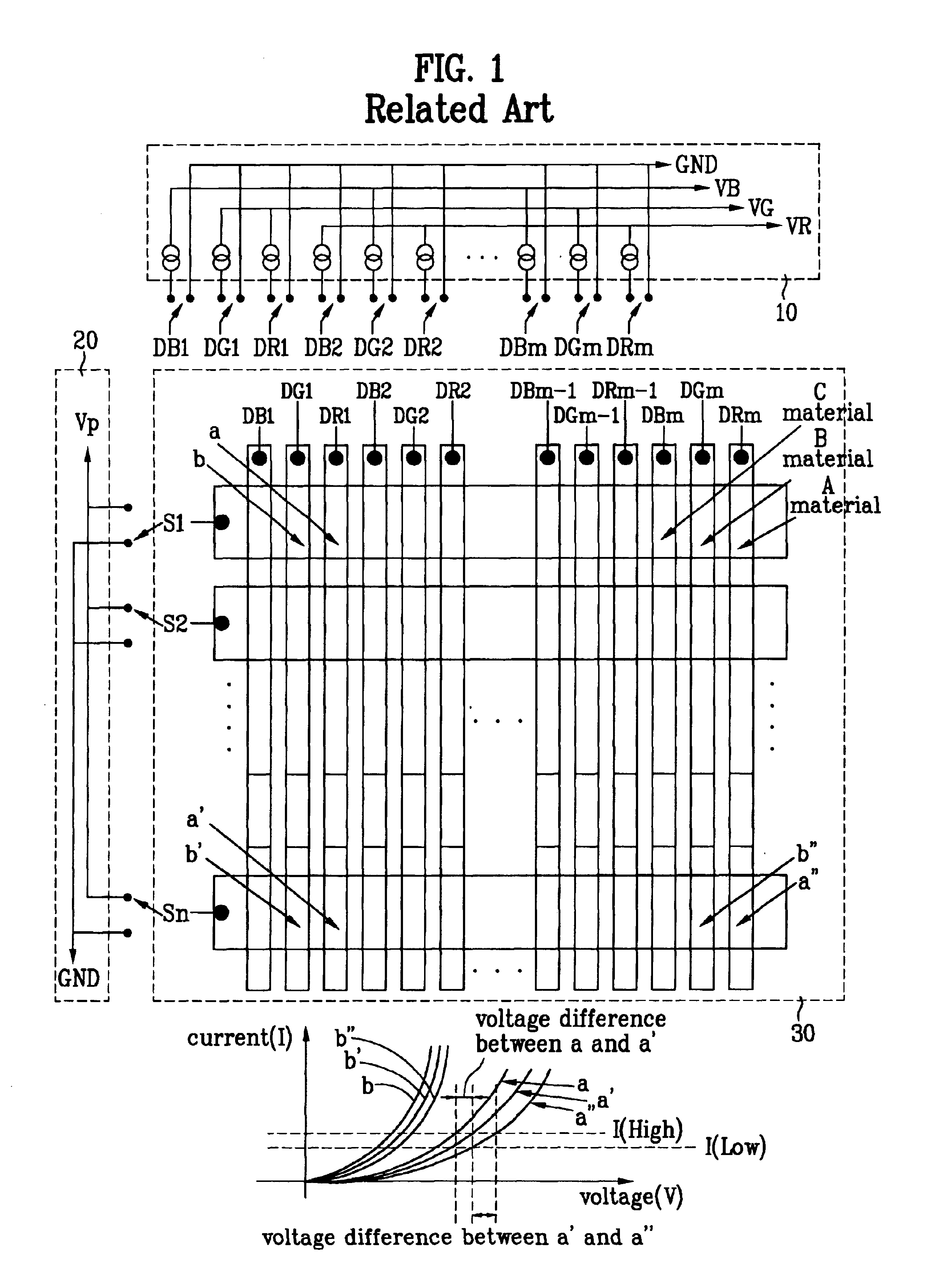
FIG. 10 shows a driving circuit for an organic EL device having an array structure according to the third embodiment of the invention.

Referring to FIG. 10, the driving circuit is comprised of an anode circuit 301 for applying a certain drive voltage to each of light emitting RGB pixels, a cathode circuit 302 for outputting scan signals to the cathode lines with both ends of cathode lines being connected in a circuit, and a display unit 303 for being displayed by data signals and the scan signals through the adjustment of the area ratio of each of the RGB light emitting pixels and the width of the anode lines according to the features of a drive voltage applied to each of the light emitting RGB pixels.

Hereinafter, the current driven organic EL device of the invention as shown in FIG. 10 will be compared with the EL device of the related art as shown in FIG. 1.

If the different value of drive voltage is outputted from the anode circuit 10 for each of the RGB pixels as in the circuit of...


PUM


Abstract

Disclosed is a full color flat display panel by using an organic electro-luminescent(EL) device, a manufacturing method thereof and a driving circuit of the organic EL device, in particular, which includes first, second and third pixels, a plurality of first electrodes, and a plurality of second electrodes perpendicularly intersecting the first electrodes, in which each of the first, second and third light emitting pixels is arranged in each of intersecting positions of the first and second electrodes. Light emitting pixels are arranged to have different areas according to luminous efficiency so that a red light emitting area with relatively poorer efficiency is sized larger than a blue or green light emitting area thereby manufacturing an efficient full color organic EL display panel. Also, the influence from the line resistance in the anode lines and the cathode lines is reduced when a constant current is introduced into the device structured of the RGB array in order to realize the white light as full color. Thus, the voltage loss on the line resistance is prevented and the area ratio of the device is adjusted to make each of the RGB pixels for generating the white light have the similar value of drive voltage thereby minimizing power loss.

Description

BACKGROUND OF THE INVENTION1. Field of the InventionThe present invention relates to a full color flat display panel by using an organic electro-luminescent(EL) device, a manufacturing method thereof and a driving circuit of the organic EL device.2. Description of the Related ArtLately, the flat display industry has been remarkably developed. In particular, an organic EL array is gradually gaining interest as an image source in a direct display or a virtual display since the organic EL array can generate a relatively large amount of light and a display adopting the organic EL array can be used under various surrounding conditions.In other words, the organic EL array can emit light in a sufficient amount so as to be used as the display under the various surrounding conditions ranging from those with no or little amount of light to those with sufficient amount of light.Also, the organic EL array can be manufactured in a low price, and variously applied from a very small size of under ...

Claims


Application Information

Patent Timeline
IPC IPC(8): H01L27/32H01L27/28
CPCH01L27/3211H01L27/3281H01L51/5212H01L51/5203H01L27/329G09G3/3216G09G2300/0426H10K59/352H10K59/353H10K59/17H10K59/1795H10K50/813H10K50/814
Inventor KIM, CHANG NAMKIM, HAK SUKIM, JUNG BAEKIM, MYUNG SEOP
Owner LG ELECTRONICS INC
Why Eureka
Try Eureka