Method of manufacturing an organic electroluminescent device and resulting device

Inactive Publication Date: 2006-08-22
SANYO ELECTRIC CO LTD
View PDF7 Cites 5 Cited by
  • Summary
  • Abstract
  • Description
  • Claims
  • Application Information

AI Technical Summary

Benefits of technology

[0007]The present invention has been made in view of the foregoing circumstances and an object thereof is to provide a technology for reducing the occurrences of poor luminescence in an organic EL device.
[0008]A preferred embodiment according to the present invention relates to a method of manufacturing an organic electroluminescent device. This method is one for manufacturing an organic electroluminescent device by depositing an organic layer on a substrate. The organic layer is deposited so as to cover foreign particles adhering to the surface of the substrate substantially. The organic layer may include deposited layers of organic-containing materials, such as a luminescent layer, a hole transporting layer, and an electron transporting layer. Since the foreign particles are substantially covered with the organic layer, it is possible to avoid a short between the anode and the cathode, thereby reducing poor luminescence. All the adhering foreign particles are preferably covered with the organic layer, whereas not all the adhering foreign particles necessarily cause an interelectrode short. For example, in the case of an organic EL panel having a plurality of organic EL devices, foreign particles need only be covered such that an upper limit to the number of dead pixels in a panel for products to satisfy, if specified, is not exceeded. It is essential only that the organic layer is deposited to such a thickness as is expected sufficient to reduce the number of occurrences of poor luminescence ascribable to interelectrode shorts to the allowable range.

Problems solved by technology

When poor luminescence occurs for any reason, however, dead pixels appear on-screen with deterioration in screen visibility, sometimes presenting an obstacle to the display function.
It has therefore been a significant challenge to ascertain the cause of the poor luminescence and prevent it effectively so that organic EL displays having fewer dead pixels or no dead pixel can be fabricated with high yield.

Method used


Image

  • Method of manufacturing an organic electroluminescent device and resulting device
  • Method of manufacturing an organic electroluminescent device and resulting device
  • Method of manufacturing an organic electroluminescent device and resulting device

Examples


first embodiment

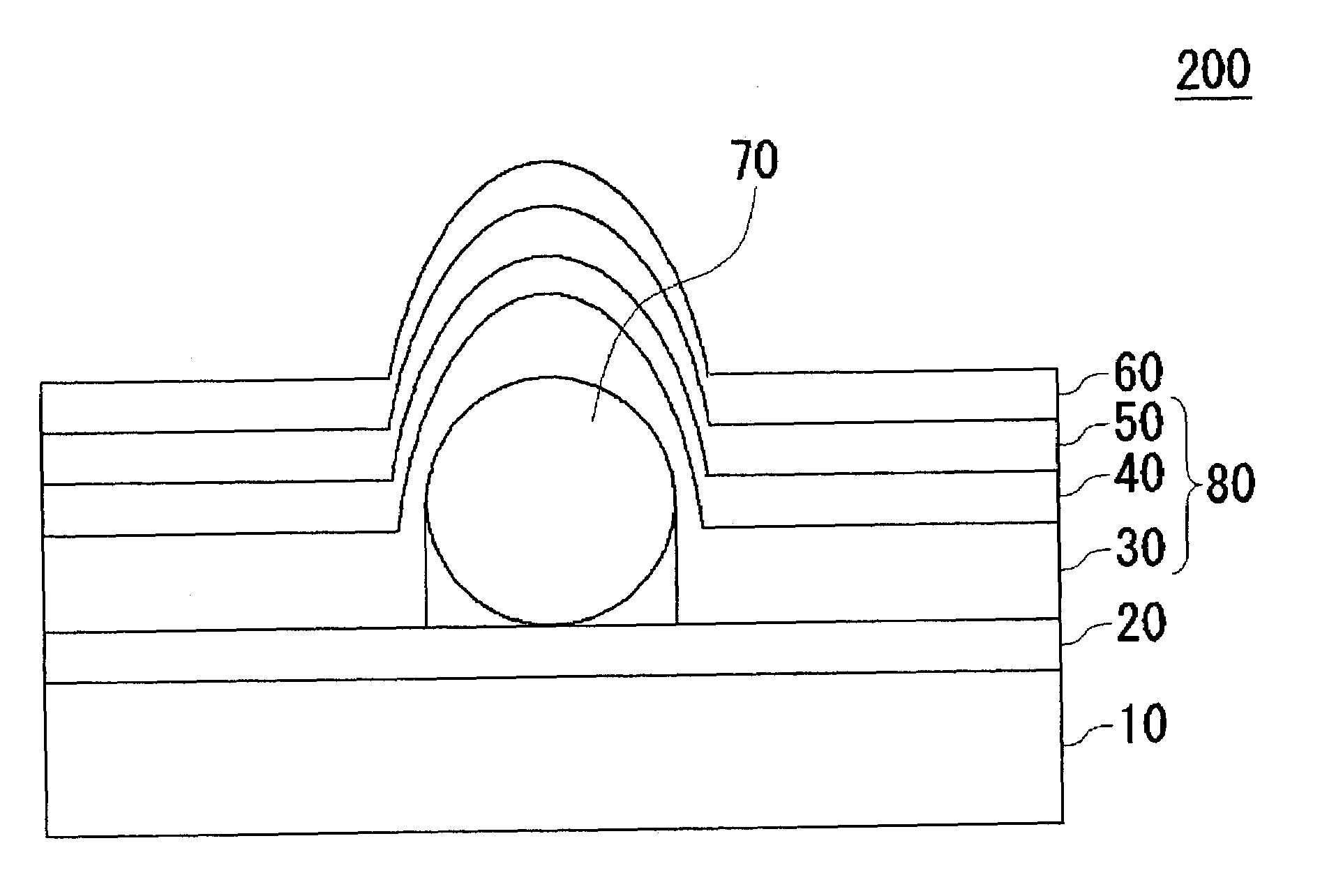
[0034]FIG. 3 schematically shows the sectional structure of an organic EL device according to a first embodiment of the present invention. In the present embodiment, the hole transporting layer 30 is increased in thickness so that the foreign particle 70 is substantially covered with the hole transporting layer 30.

[0035]A substrate 10 is made of an insulative substance such as glass. In the case of an active matrix type organic EL panel, for example, the substrate 10 has the structure in which driving circuits containing switching elements such as TFTs are formed on an insulative substrate, and a planarization film and the like are formed thereon. As employed in this specification, the substrate 10 shall also include such configuration as the driving circuits.

[0036]An anode layer 20 is formed on the substrate 10. The anode layer 20 is made of such material as indium tin oxide (ITO), tin oxide (SnO2), or indium oxide (In2O3). ITO is typically used because of its hole injection effici...

second embodiment

[0046]FIG. 8 schematically shows the sectional structure of an organic EL device according to a second embodiment. In the present embodiment, the electron transporting layer 50 is increased in thickness so that the foreign particle 70 is substantially covered with the electron transporting layer 50.

[0047]As shown in FIG. 8, even if the hole transporting layer 30 and the luminescent layer 40 fail to cover the foreign particle 70 adhering on the anode layer 20, the electron transporting layer 50 deposited thickly can substantially cover the foreign particle 70 to avoid electric contact between the anode and the cathode. Here, as with the thickness of the hole transporting layer 30 in the first embodiment, the thickness of the electron transporting layer 50 is desirably 1300 angstroms or above, and preferably 1700 angstroms or above. The upper limit to the thickness of the electron transporting layer 50 need only be designed not to have much effect on the characteristics of the organic...

third embodiment

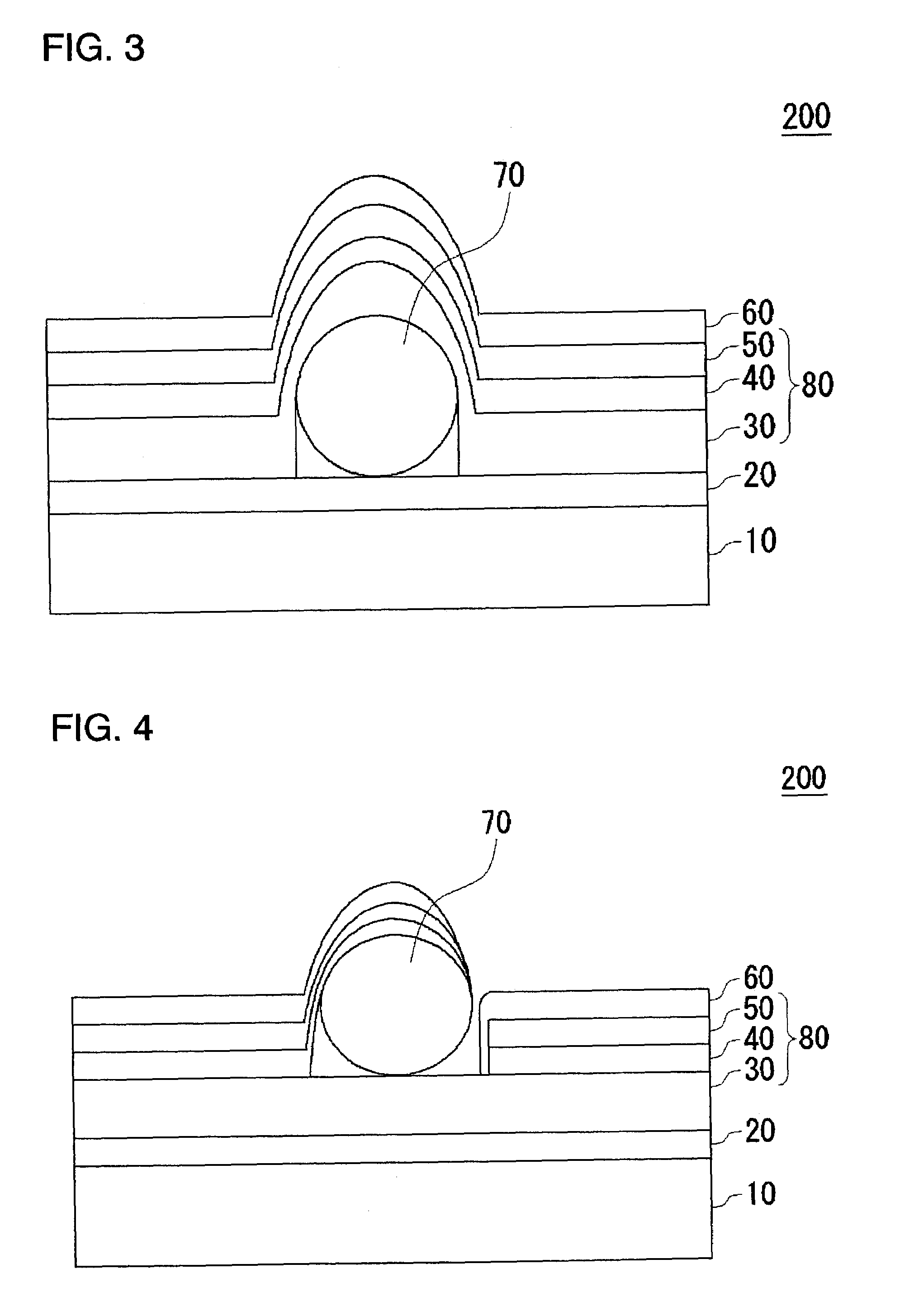
[0048]FIG. 9 schematically shows the sectional structure of an organic EL device according to a third embodiment. The organic EL device of the present embodiment has the electrode layers at positions opposite from in the organic EL devices of the first and second embodiments. The substrate 10 is covered with the cathode layer 60, on which the electron transporting layer 50, the luminescent layer 40, the hole transporting layer 30, and the anode layer 20 are laminated in this order. As shown in FIG. 9, the electron transporting layer 50 lying immediately above the cathode layer 60 can substantially cover the foreign particle 70 adhering on the cathode layer 60, thereby preventing an interelectrode short and avoiding poor evaporation of the luminescent layer 40.

[0049]Here, as with the thickness of the hole transporting layer 30 in the first embodiment, the thickness of the electron transporting layer 50 is desirably 1300 angstroms or above, and preferably 1700 angstroms or above. The ...


PUM


Abstract

An organic EL device is fabricated by a novel method to reduce the occurrence of poor luminescence in the organic EL device. An anode layer, a hole transporting layer, a luminescent layer, an electron transporting layer, and a cathode layer are laminated in this order on a substrate to form an organic EL device. In the organic EL device, the hole transporting layer is increased in thickness so that foreign particles adhering on the anode layer are substantially covered with the hole transporting layer.

Description

BACKGROUND OF THE INVENTION[0001]1. Field of the Invention[0002]The present invention relates to an organic electroluminescent device and a method of manufacturing the organic electroluminescent device, and more particularly to a technology for solving a problem of a defect of luminescence in an organic electroluminescent device.[0003]2. Description of the Related Art[0004]Organic electroluminescent displays (hereinafter, also referred to as “organic EL displays” or “organic EL panels”) are attracting attention as new flat-type displays. In particular, active matrix type organic EL displays having thin film transistors (hereinafter, also referred to as “TFTs”) as switching elements are regarded as sweeping out the currently prevailing liquid crystal displays in the near future, and are in a fierce development race for practical application.[0005]FIG. 1 schematically shows the sectional structure of a typical organic electroluminescent device (hereinafter, also referred to as “organi...

Claims


Application Information

Patent Timeline
IPC IPC(8): H05B33/00H01L51/50H05B33/10
CPCH01L51/5048H01L51/5012H10K50/14H10K50/11H05B33/10
Inventor MATSUKI, HIROSHINISHIO, YOSHITAKA
Owner SANYO ELECTRIC CO LTD
Why Eureka
Try Eureka