Enhanced CPLD macrocell module having selectable bypass of steering-based resource allocation

a macrocell module and selectable bypass technology, applied in the field of monolithic integrated circuits, can solve problems such as failure to complete the mission on the first try

Inactive Publication Date: 2005-01-04
LATTICE SEMICON CORP
View PDF5 Cites 21 Cited by
  • Summary
  • Abstract
  • Description
  • Claims
  • Application Information

AI Technical Summary

Benefits of technology

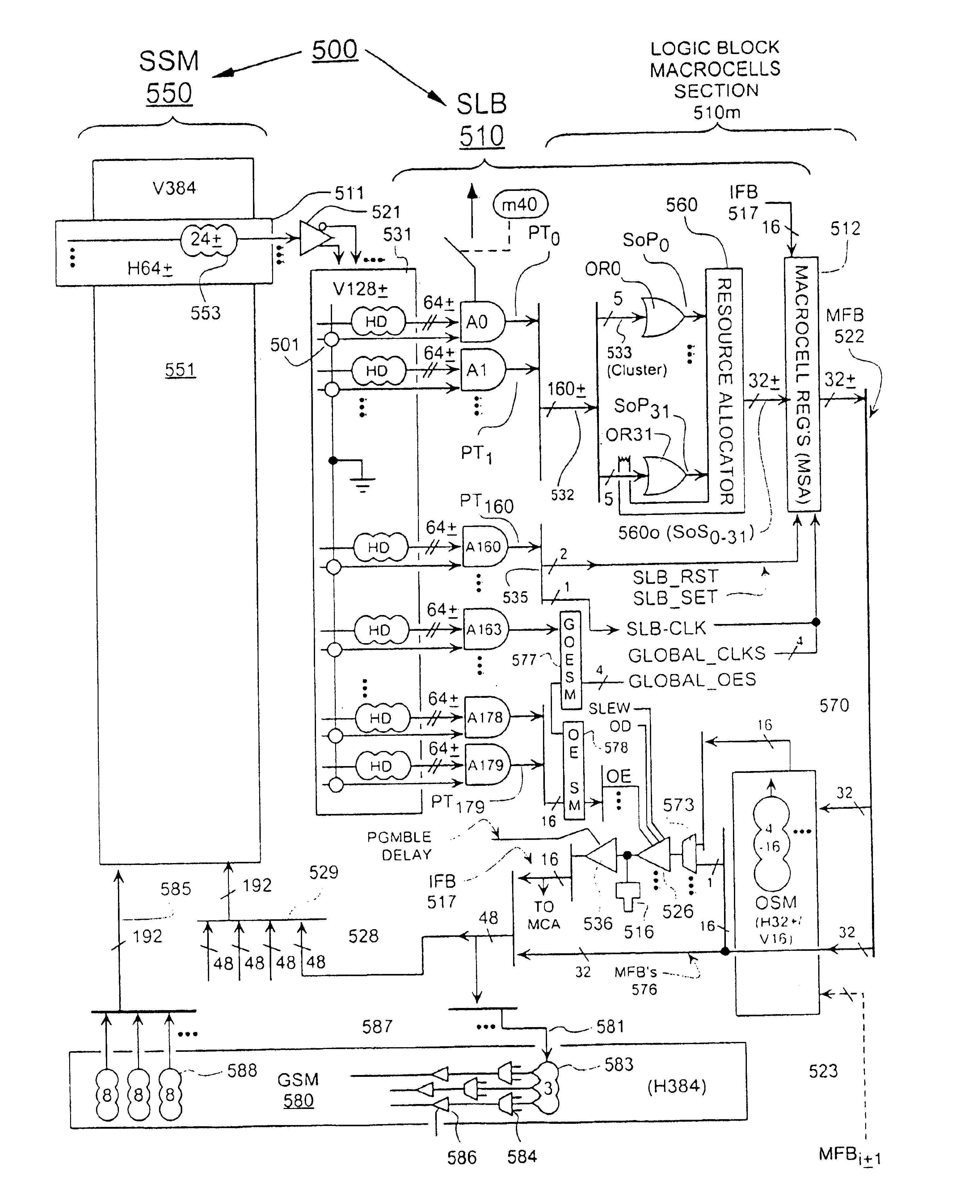
(B) In accordance with a second aspect of the present disclosure, techniques are provided for concentrating the development of complex function signals (e.g., ≦80PT's) within singular logic blocks so that the development of such complex function signals does not consume inter-block interconnect resources.

Problems solved by technology

In various instances, the CPLD configuring software may find that it cannot complete its mission successfully on a first try.
Moreover, if the CPLD does not have enough resources, the CPLD configuring software may find that it has exhausted CPLD resources (e.g., inter-block interconnect) without completing the to-be-implemented design.

Method used


Image

  • Enhanced CPLD macrocell module having selectable bypass of steering-based resource allocation
  • Enhanced CPLD macrocell module having selectable bypass of steering-based resource allocation
  • Enhanced CPLD macrocell module having selectable bypass of steering-based resource allocation

Examples


second embodiment

Multiplexer 753 of the second embodiment optionally further receives the MFBJ signal as an input via line 722d. This option allows for re-registration of the MFBJ signal (see register output 722 of FIG. 7B) or optional exclusive-ORring of the MFBJ signal with a sum of SoP or SoS signals collected at inputs port 745i and thereafter provided as a sum on line 751a. Thus, the functionally-rich, sums-of-sums that is defined by output 745o of the SoS-producing gate of module J can be further enriched by selectively inverting or not inverting it as a function of the MFBJ signal output by storage / pass element 760.

The accompanying Table 2.1 shows one possible decoding option for configuration memory bits m16,13,28 of the second embodiment.

TABLE 2.1747-0747-1MUX outREG INm16m13m28(751a)(to J + 4)(751b)(751o)0000SoSJIFBIN = PAD0100SoSJLP′ IN = (PT0′)10000IFBIN = PAD110SoSJ0LP′IN = SoSJ(+)LP′0010SoSJSoPJIN = SoPJ0110SoSJMFBJ IN = MFBJ10100SoPJIN = SoPJ111SoSJ0MFBJIN = SoSJ(+)MFBJ

It may be appre...

embodiment 800

Referring to FIG. 8, a particular embodiment 800 for generating global output enable signals is shown. In the illustrated example, it is assumed that each bank (or segment) of the CPLD contains four logic blocks (LB's) and that the respective banks / segments are denoted as A through N. A contributions-collecting bus 801 extends through all the logic blocks for selectively collecting from the respective contribution signals (e.g., PT'82.A1 through PT′82.N4) of the respective logic blocks LB-A1 through LB-N4 in banks / segments A-N a subset of signals (GOE-candidates) for use as GOE signals (804′). Bus 801 is four lines wide in the illustrated example and thus collects a subset of four product term contributions from the fully-populated switch matrix (a PIP at each crosspoint) that links product terms gates A′82.1 through A″82.4 to contributions-collecting bus 801. Although a fully-populated switch matrix is shown on bus 801, it is also valid to use a partially-populated switch matrix in...

embodiment 302

The collected subset of 4 signals (801) may be coupled to a corresponding set of four polarity-selecting multiplexers 841-844. In one embodiment, two substitution multiplexers 821 and 822 are provided each for respectively substituting the signal of a respective I / O pin or global OE pin into the polarity-reversible mix in place of a corresponding one of two of the collected PT contribution signals. (The alternate embodiment 302 in FIG. 3B provides for full substitution of external signals (global OE pins) for internally-generated and contributed PT's 801.) An advantage of using a fewer number (e.g., 2) of I / O or global OE pins than the number (e.g., 4 on bus 804′) of global OE signals that are globally distributed in the CPLD is that pinout pin count is reduced. At least some of the global OE signals are internally derived (e.g., the outputs of multiplexers 843 and 844). As seen in FIG. 8, a first global configuration memory cell G03 controls the selection of substitution multiplexe...


PUM


Abstract

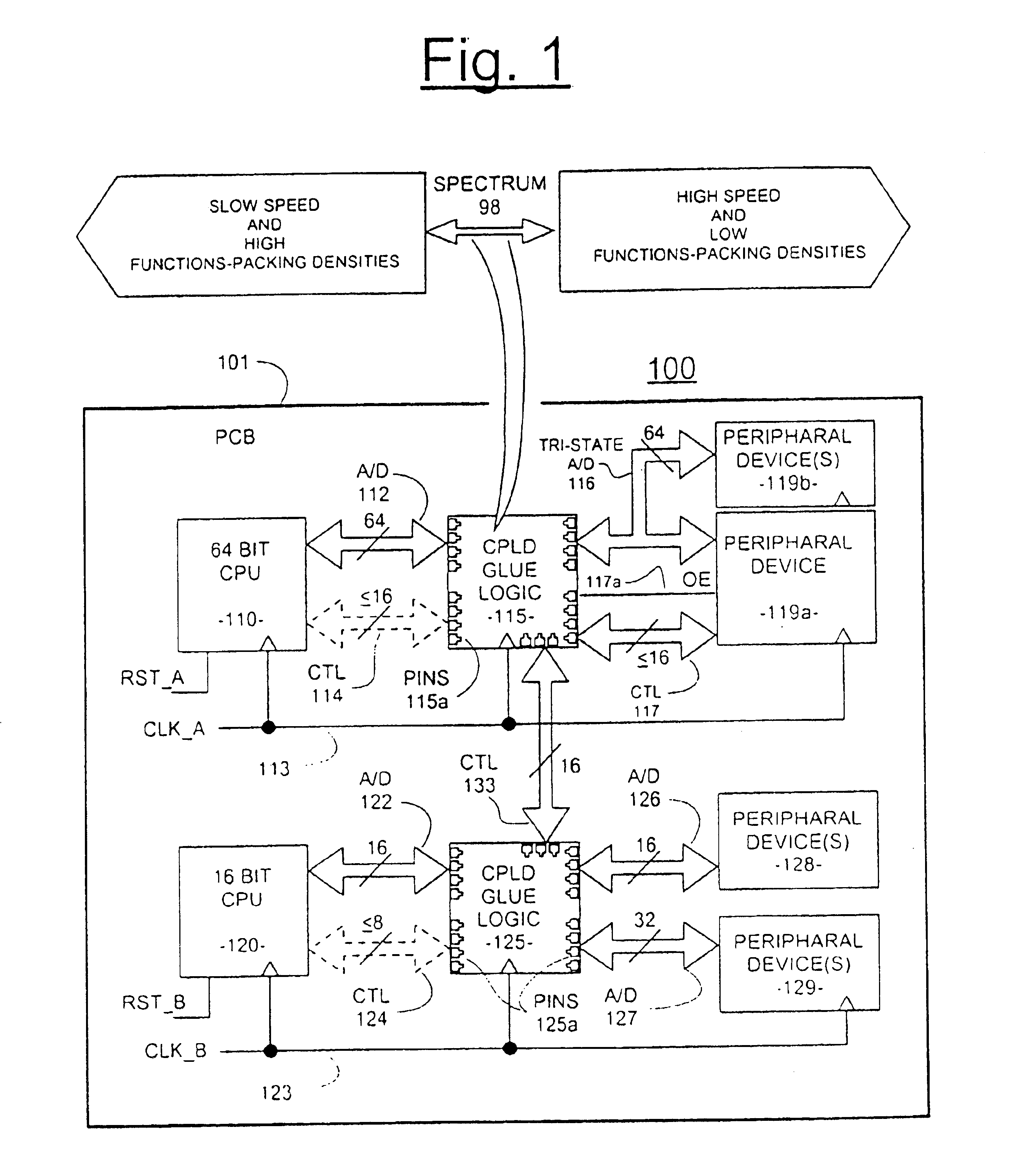
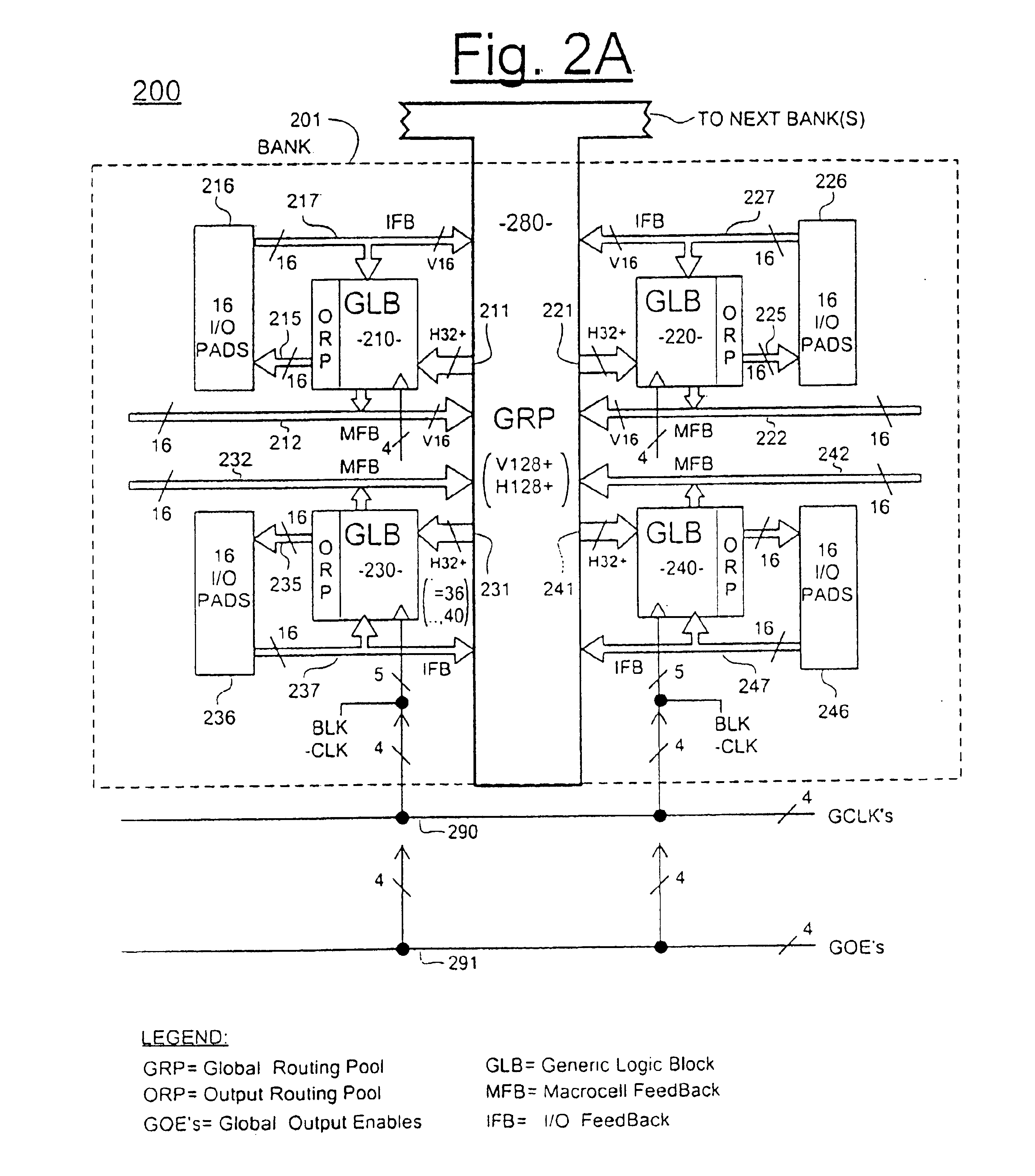
Structures and techniques are provided for allowing one or more of the following actions to occur within a Complex Programmable Logic Device (CPLD): (1) Elective use of a fast, allocator-bypassing path (e.g., a fast 5-PT path) in combination with in-block simple or super-allocation; (2) Elective use of an OSM-bypassing path for signals that do not need pin-consistency; (3) Automatic re-routing of output enable signals that corresponding to output signals which are re-routed for pin-consistency purposes; (4) Global distribution of globally-usable output enable signals; (5) Elective use of two-stage steering to develop complex sum-of-clusters terms where fast path or simple allocation will not be sufficient; and (6) Use of unidirectional super-allocation with stage-2 wrap-around in designs having about 24 or less macrocell units per logic block. Techniques are provided for concentrating the development of complex function signals (e.g., ≦80PTs) within singular logic blocks so that the development of such complex function signals does not consume inter-block interconnect resources. One CPLD configuring method includes the machine-implemented steps of first identifying middle-complexity functions that are achievable by combined simple or super-allocation based development in one logic block and fast-path completion in the same or a second logic block; and configuring the CPLD to realize one or more of the functions identified in the first identification step by simple or super-allocation based development in one logic block and fast-path completion in the same or a second logic block.

Description

FIELD OF DISCLOSUREThe present disclosure of invention relates generally to monolithic integrated circuits, and more specifically to a repeated macrocell module design for use within Programmable Logic Devices (PLD's).The disclosure relates even more specifically to a macrocell module design as applied to a subclass of PLD's known as Complex Programmable Logic Devices (CPLD's) and High-Density Complex Programmable Logic Devices (HCPLD's).CROSS REFERENCE TO CO-OWNED APPLICATIONSThe following copending U.S. patent applications is owned by the owner of the present application, and its disclosure is incorporated herein by reference:(A) Ser. No. 09 / 927,793 filed Aug. 10, 2001 by Om P. Agrawal et al. and which was originally entitled, “Enhanced Macrocell Module Having Expandable Product Term Sharing Capability For Use in High Density CPLD Architectures”.CROSS REFERENCE TO PATENTSThe disclosures of the following U.S. patents are incorporated herein by reference:(A) U.S. Pat. No. 6,150,841 ...

Claims


Application Information

Patent Timeline
Patent Type & Authority Patents(United States)
IPC IPC(8): H03K19/177
CPCH03K19/17728H03K19/17748H03K19/17736
Inventor AGRAWAL, OM P.FONTANA, FABIANOBOSCO, GILLES M.
Owner LATTICE SEMICON CORP
Why Eureka
Try Eureka