Method of manufacturing a semiconductor device having a silicide film
- Summary
- Abstract
- Description
- Claims
- Application Information
AI Technical Summary
Benefits of technology
Problems solved by technology
Method used
Image

Examples
first embodiment
(First Embodiment)
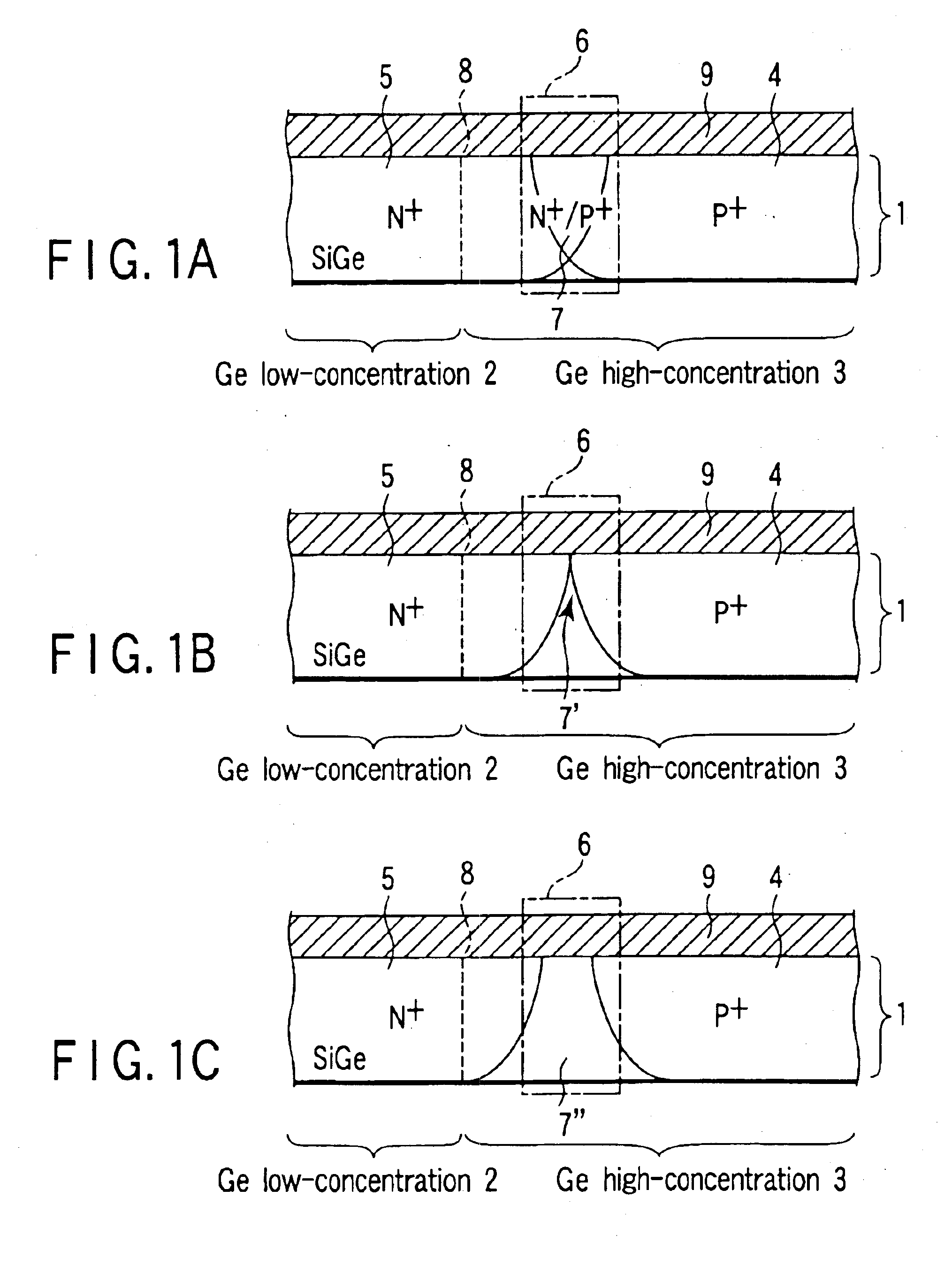
FIG. 1A is a cross sectional view showing a semiconductor device according to a first embodiment of the present invention.
As shown in FIG. 1A, silicon (Si) and germanium (Ge) are contained in a semiconductor region, for example, in a semiconductor film 1. One example of the semiconductor film l is the gate pattern of a MOSFET. A Ge low-concentration region 2 in which germanium is contained with low concentration and a Ge high-concentration region 3 in which germanium is contained with high concentration are formed in the semiconductor film 1 in the present embodiment.
Further, in the semiconductor film 1, a P+ diffusion layer 4 and N+ diffusion layer 5 are formed. A boundary region 6 between the P+ diffusion layer 4 and the N+ diffusion layer 5 is formed in the Ge high-concentration region 3.
The boundary region 6 in the present embodiment contains an impurity mixture region (N+ / P+) 7 containing N-type and P-type impurities. The P+ diffusion layer 4 is formed in the ...
second embodiment
(Second Embodiment)
The second embodiment is associated with an example of a case wherein the first embodiment is applied to a CMOS semiconductor device.
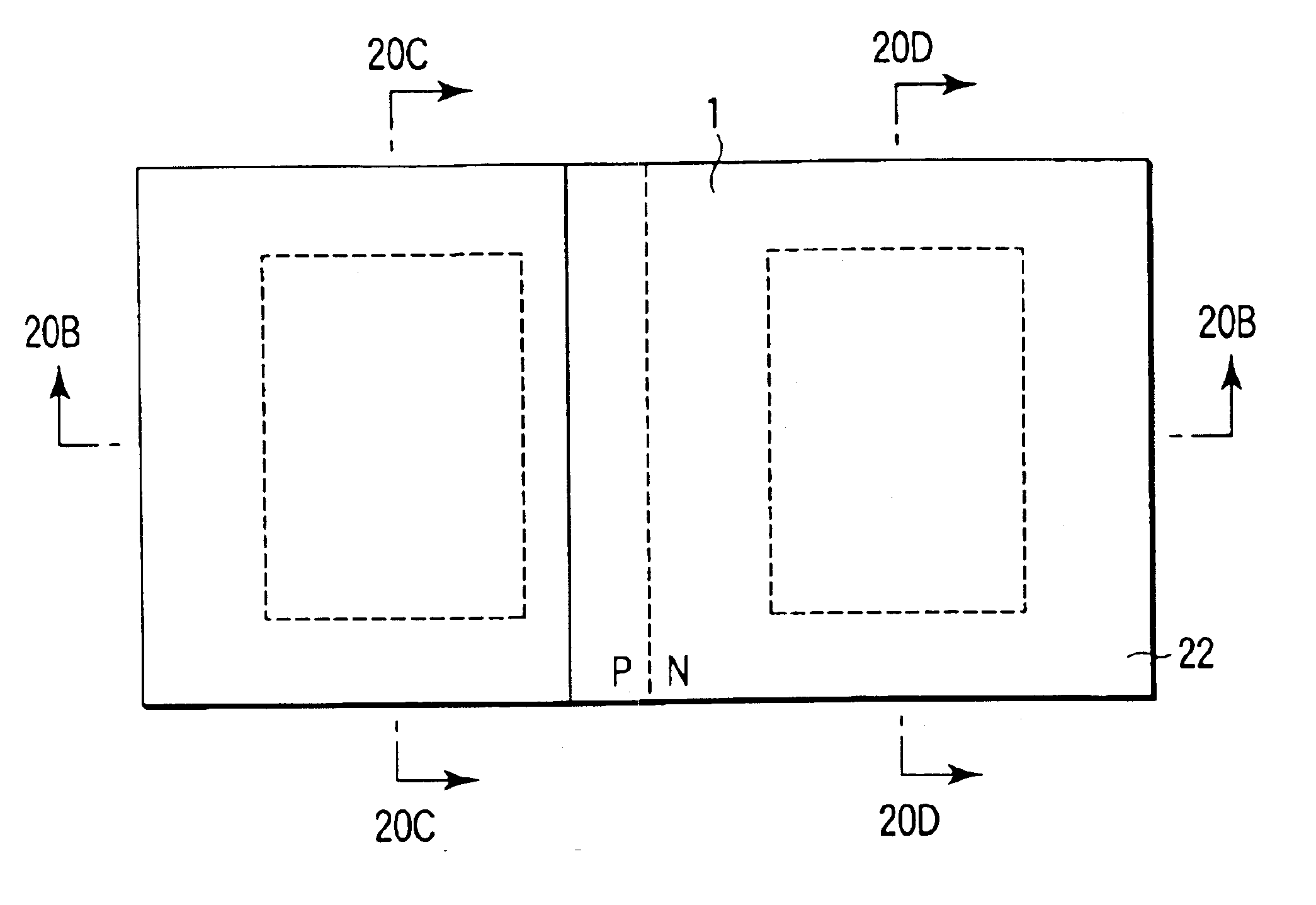
FIG. 14A is a plan view showing a semiconductor device according to the second embodiment of the present invention, FIG. 14B is a cross sectional view taken along the 14B—14B line of FIG. 14A, FIG. 14C is a cross sectional view taken along the 14C—14C line of FIG. 14A, and FIG. 14D is a cross sectional view taken along the 14D—14D line of FIG. 14A.
The semiconductor device according to the second embodiment is explained according to one example of the manufacturing method below.
FIGS. 15A to 15D, . . . FIGS. 28A to 28D are plan views or cross sectional views showing the semiconductor device of the first embodiment according to one example of the manufacturing method.
First, as shown in FIGS. 15A to 15D, a P-type semiconductor region 20 in which a first transistor is to be formed and an N-type semiconductor region 21 in which a second tr...
third embodiment
(Third Embodiment)
Like the second embodiment, the third embodiment is associated with an example of a case wherein the first embodiment is applied to a CMOS semiconductor device.
FIG. 29A is a plan view showing a semiconductor device according to the third embodiment of the present invention, FIG. 29B is a cross sectional view taken along the 29B—29B line of FIG. 29A, FIG. 29C is a cross sectional view taken along the 29C—29C line of FIG. 29A, and FIG. 29D is a cross sectional view taken along the 29D—29D line of FIG. 29A.
As shown in FIGS. 29A to 29D, the third embodiment is similar to the second embodiment except that an SiGe substrate containing silicon and germanium is used as a substrate 19, a Ge low-concentration region 2′ containing germanium of low concentration and a Ge high-concentration region 3′ containing germanium of high concentration are formed on the SiGe substrate, an N-type semiconductor region 21 on which P+ diffusion layers 24P are formed is formed in the Ge high-...
PUM
 Abstract
Description
Claims
Application Information