Dynamic method for limiting the reverse base-emitter voltage

a reverse base-emitter and voltage limit technology, applied in pulse manipulation, gated amplifiers, pulse techniques, etc., can solve the problems of -degradation and increased noise, increase in noise,

Inactive Publication Date: 2005-01-18
ANALOG DEVICES INC
View PDF5 Cites 1 Cited by
  • Summary
  • Abstract
  • Description
  • Claims
  • Application Information

AI Technical Summary

Benefits of technology

In a circuit having two input stages multiplexed to a common output stage having an output, one of the two input stages including transistor having a base, a collector and an emitter; a method of protecting the transistor from μ-degradation when the one of the two input stages is disabled comprises: clamping the base to a substantially fixed voltage for a first range of voltages applied to the one of the two input stages; and bootstrapping the base to a voltage that follows the output for a second range of voltages applied to the one of the two input stages. The method may further comprise applying a reference voltage through a series resistance to a buffer amplifier having an output connected to the base. The method may yet further comprise injecting a current into the series resistance, the injected current proportional to the voltage applied to the one of the two input stages. The method may even yet further comprise providing the series resistance by simulating a large resistor using an operational transconductance amplifier. Alternatively, the method may further comprise defining the first range of voltages and the fixed voltage so a reverse Vbe of the transistor never exceeds a voltage at which μ-degradation is observable.
Alternatively, a method of protecting a transistor having a base connected through a finite impedance to an input voltage, a collector and an emitter, may comprise bootstrapping the base to a voltage that follows the input voltage with an offset when the input voltage is within a second range of voltages. This method may further comprise applying a reference voltage through a series resistance to a buffer amplifier having an output connected to the base. This method may yet further comprise injecting a current into the series resistance, the injected current proportional to the voltage applied to the one of the two input stages. This method may even yet further comprise providing the series resistance by simulating a large resistor using an operational transconductance amplifier. Alternatively, this method may further comprise defining the first range of voltages and the fixed voltage so a reverse Vbe of the transistor never exceeds a voltage at which μ-degradation is observable.
A circuit having an input voltage connected thereto through a finite impedance may comprise: a transistor having a base, a collector and an emitter; a comparator having a comparator output and having an input connected between the base and the input voltage; a clamping circuit having an output connected to the base and an input connected through a series resistance to a clamping reference voltage; and a bootstrapping circuit responsive to the comparator output, the bootstrapping circuit having an output that injects a variable current into the series resistance, altering the behavior of the clamping circuit from a fixed voltage clamp to a follower. The circuit may further comprise an operational transconductance amplifier connected to provide the series resistance. The circuit may yet further comprise a transconductance amplifier that produces the variable current; and a current mirror operatively connected to mirror the variable current into the series resistance.

Problems solved by technology

In particular, the application relates to protection of bipolar transistors from excess reverse Vbe voltages, including those resulting in μ-degradation over time.
This reverse leakage current or reverse conduction causes hot carrier induced oxide damage to the oxide overlying the junction, resulting in μ-degradation and increased noise.
Hot carrier induced oxide damage results in electron migration into the oxide, creating undesired additional current paths, reducing breakdown voltage and causing the increase in noise.
Although many circuit designs do not produce voltages across the base-emitter junction, Vbe, that result in μ-degradation, there are other circuits for which this problem will occur during normal circuit operation.
Indeed, in transconductance stages including a differential pair, regardless of what mechanism causes the inputs to be very different, the fact that they are different causes the problem discussed.

Method used


Image

  • Dynamic method for limiting the reverse base-emitter voltage
  • Dynamic method for limiting the reverse base-emitter voltage
  • Dynamic method for limiting the reverse base-emitter voltage

Examples


Embodiment Construction

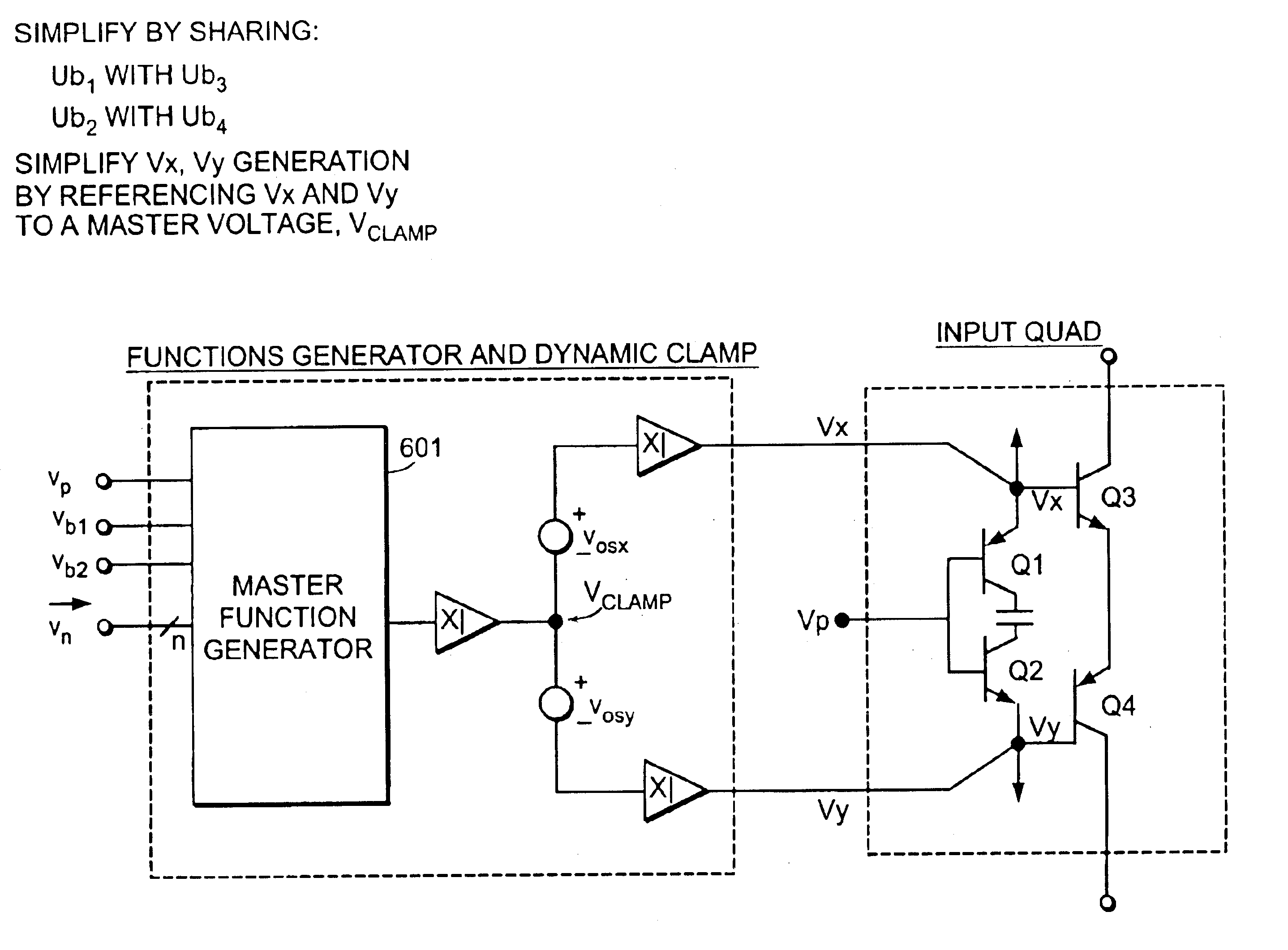
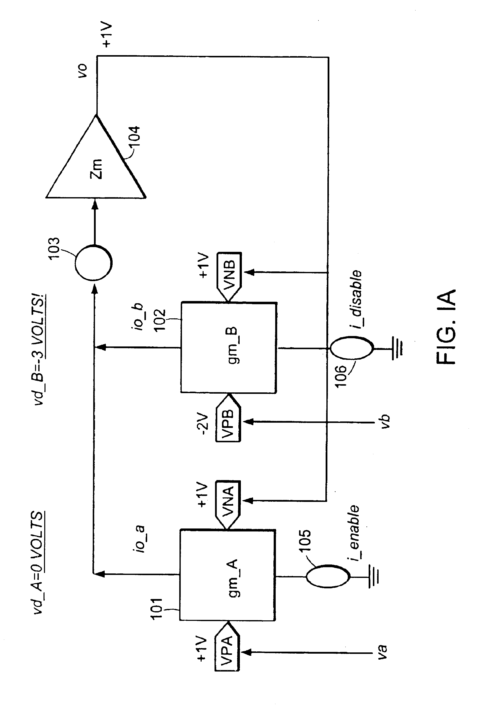
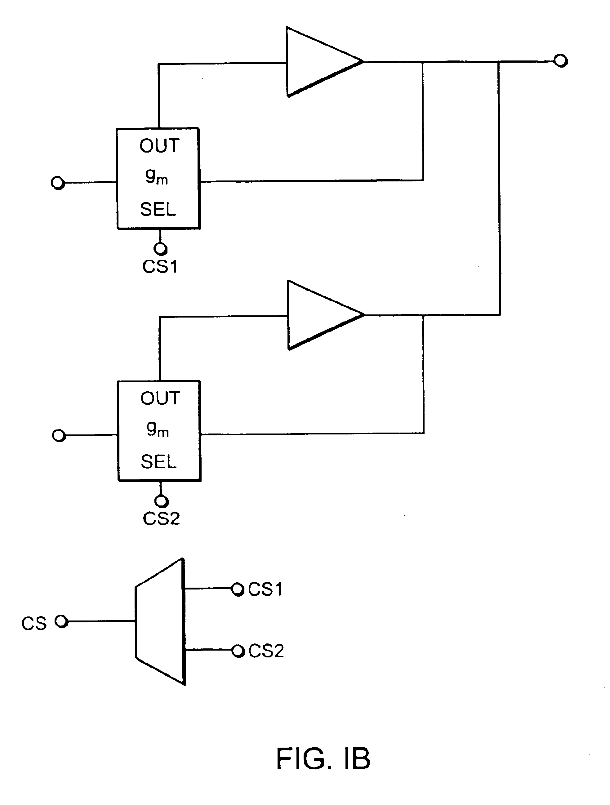
The present invention will be better understood upon reading the following detailed description of various embodiments of aspects thereof, taken in connection with the figures. The particular aspects and embodiments of the invention described relate to the two-input, transconductance multiplexer of FIG. 1A described in the background hereof. However, the invention is not limited to that application, as will be understood by those skilled in this art. Any transistor, for example those of the circuit of FIG. 1B and others, for which μ-degradation may be a problem, used in a circuit for which the methods and circuits described are suitable can be protected by application of appropriate aspects of the invention. The circuits illustrated in FIGS. 1A and 1B are non-limiting examples, only. The number of parallel input blocks (e.g., FIG. 1A, input amplifiers 101 and 102) and the number of gain stages within each input block can be varied, including the use of two or more input blocks and t...


PUM


Abstract

In a circuit having two input stages multiplexed to a common output stage having an output, one of the two input stages including transistor having a base, a collector and an emitter; a method of protecting the transistor from μ-degradation when the one of the two input stages is disabled comprises: clamping the base to a substantially fixed voltage for a first range of voltages applied to the one of the two input stages; and bootstrapping the base to a voltage that follows the output for a second range of voltages applied to the one of the two input stages. Alternatively, a method of protecting a transistor having a base connected through a finite impedance to an input voltage, a collector and an emitter, may comprise bootstrapping the base to a voltage that follows the input voltage with an offset when the input voltage is within a second range of voltages. A circuit having an input voltage connected thereto through a finite impedance may comprise: a transistor having a base, a collector and an emitter; a comparator having a comparator output and having an input connected between the base and the input voltage; a clamping circuit having an output connected to the base and an input connected through a series resistance to a clamping reference voltage; and a bootstrapping circuit responsive to the comparator output, the bootstrapping circuit having an output that injects a variable current into the series resistance, altering the behavior of the clamping circuit from a fixed voltage clamp to a follower.

Description

BACKGROUND OF INVENTIONThis application relates generally to circuits for protecting transistors from adverse applied voltages. In particular, the application relates to protection of bipolar transistors from excess reverse Vbe voltages, including those resulting in μ-degradation over time.The phenomenon of μ-degradation is a response of a bipolar transistor to a stress. A bipolar transistor is a three-terminal amplifying device, whose terminals are referred to as the base, the collector and the emitter. There are junctions between the materials of which the base and collector are formed and between the materials of which the base and emitter are formed. The amount of gain, i.e. how large is the amplifying factor of the device, is called μ, hence degradation of the gain in response to a stress is called μ-degradation.The phenomenon of μ-degradation occurs when a bipolar transistor is stressed by a reverse Vbe voltage in a range between zero volts and the reverse breakdown voltage of...

Claims


Application Information

Patent Timeline
Patent Type & Authority Patents(United States)
IPC IPC(8): H03F1/52H03F3/72H03F3/45H03F3/30
CPCH03F1/52H03F3/72H03F3/45475H03F3/3076
Inventor BANKMAN, JESSE R.TAM, KIMO Y. F.
Owner ANALOG DEVICES INC
Why Eureka
Try Eureka