

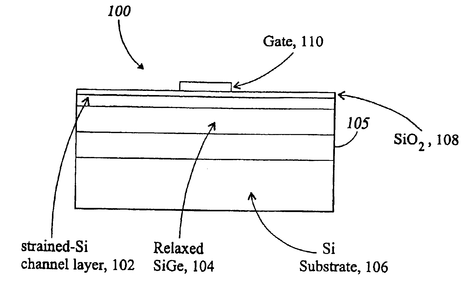
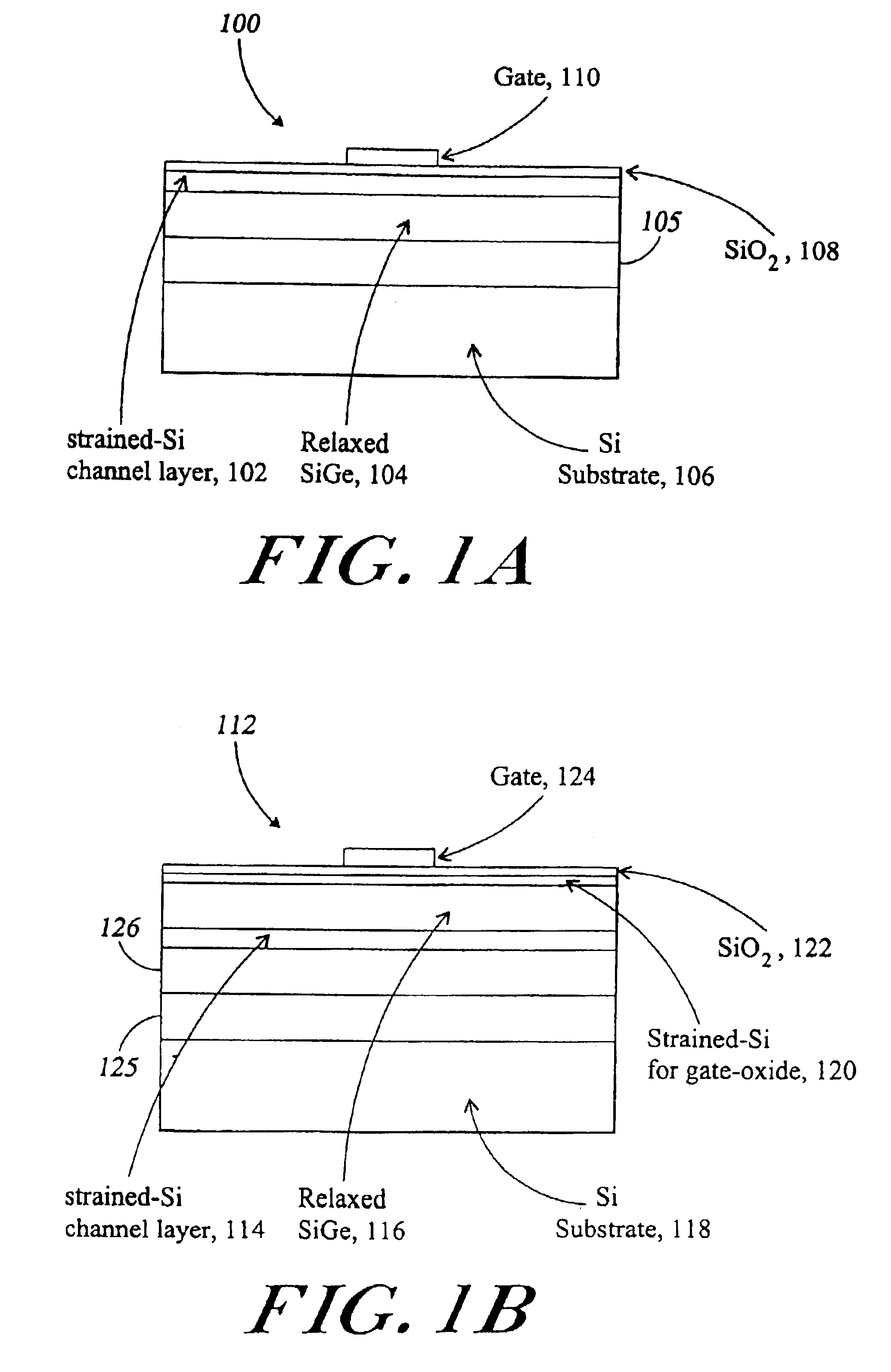
Gate technology for strained surface channel and strained buried channel MOSFET devices
a technology of mosfet and surface channel, which is applied in the direction of basic electric elements, semiconductor devices, electrical apparatus, etc., can solve the problems of consuming si material, and affecting the efficiency of the devi
- Summary
- Abstract
- Description
- Claims
- Application Information
AI Technical Summary
Benefits of technology
Problems solved by technology
Method used
Image

Examples
Embodiment Construction
To eliminate the issue of losing valuable surface Si, an innovative step that has not been previously considered can be employed. In fact, any interest in this area is dominated by discussions of how to change the Si device and circuit process to conserve Si consumption. Although these are certainly possibilities, such constraints severely limit process flexibility, alter the process further from the conventional Si process, and most likely will increase the cost of the fabrication process.
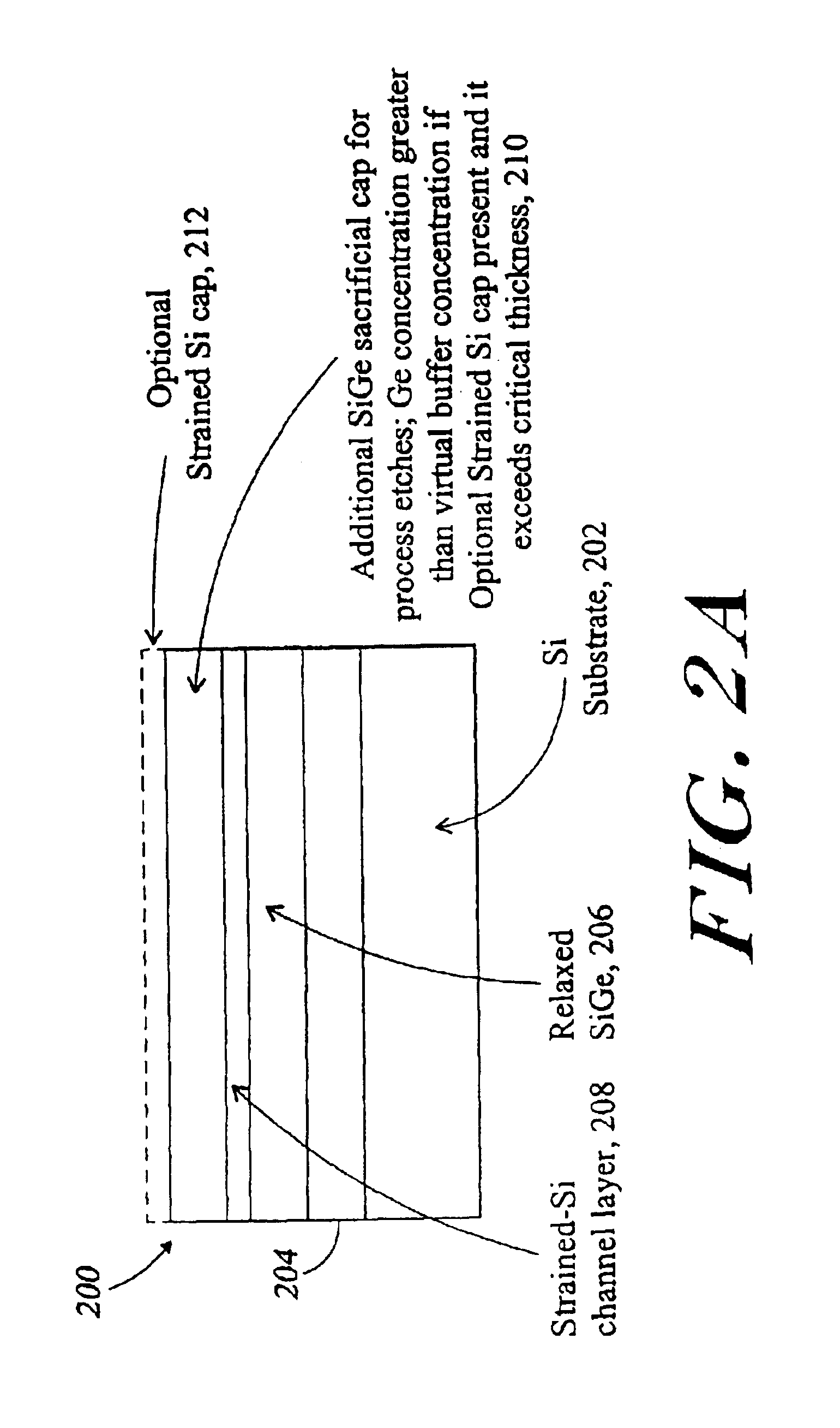
A solution for the buried channel and surface channel structures is to actually deposit another SiGe layer after the desired device structure (which, in the buried channel heterostructure, includes the sacrificial Si layer for oxidation). The structures are shown in FIGS. 2A and 2B.
FIG. 2A is a cross section of a block diagram of a starting heterostructure 200 for surface channel strained MOS in accordance with the invention. The structure 200 includes a Si substrate 202, a SiGe graded buffer 204,...
PUM
 Abstract
Description
Claims
Application Information