

Light sensitive semiconductor package and fabrication method thereof
- Summary
- Abstract
- Description
- Claims
- Application Information
AI Technical Summary
Benefits of technology
Problems solved by technology
Method used
Image

Examples
first preferred embodiment
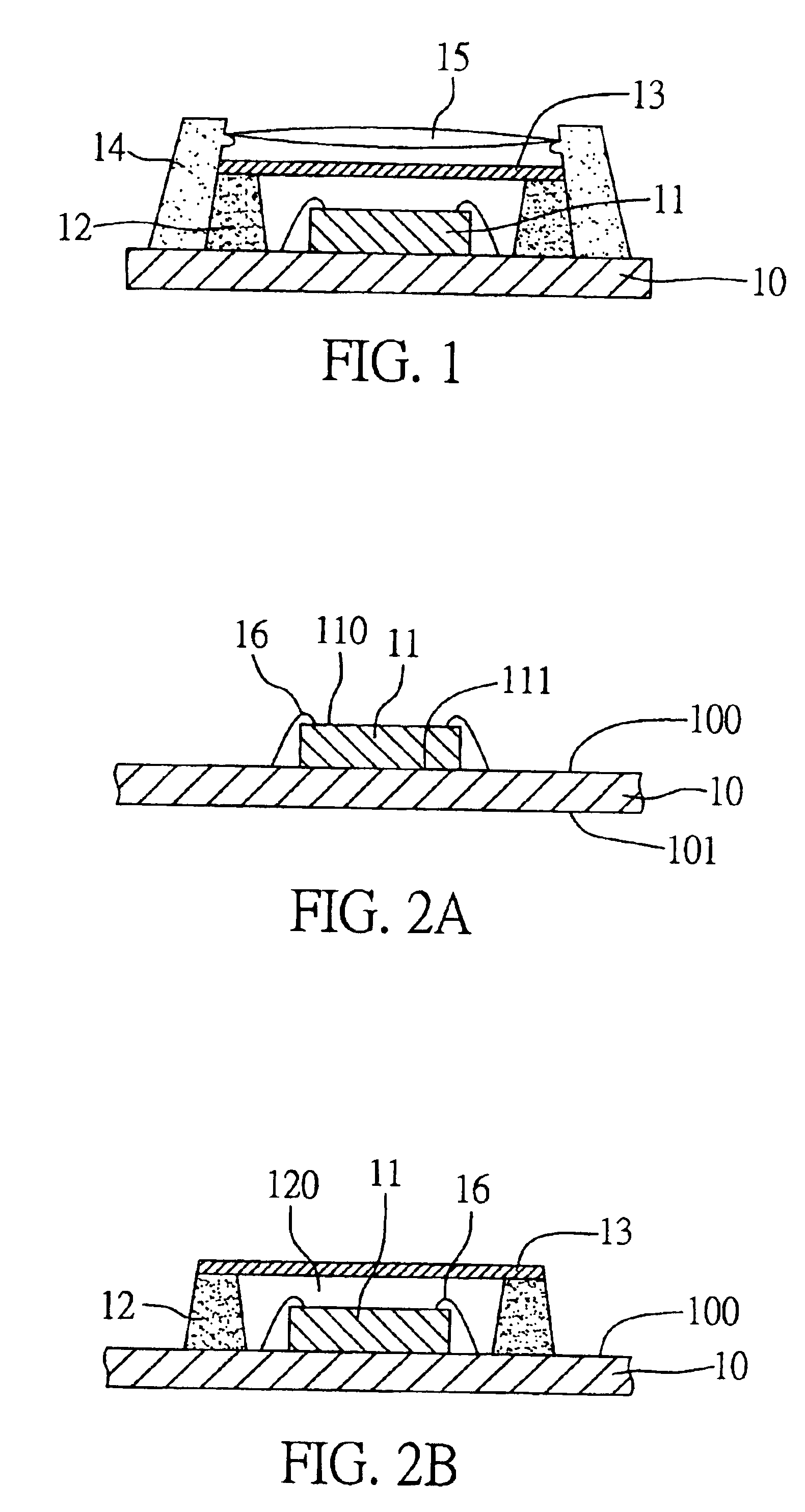
As shown in FIG. 1, a light sensitive semiconductor package according to a first preferred embodiment of the invention includes: a chip carrier 10; at least one chip 11 mounted on and electrically connected to the chip carrier 10; a dam 12 formed on the chip carrier 10 and surrounding the chip 11; a first light permeable member 13 attached to the dam 12 for hermetically isolating the chip 11 from the atmosphere; an encapsulant 14 formed on the chip carrier 10 and surrounding the dam 12; and a second light permeable member 15 supported by the encapsulant 14 and disposed above the first light permeable member 13, allowing light to penetrate through the first and second light permeable members 13, 15 to reach the chip 11 and facilitate operation of the chip 11.
The above light sensitive semiconductor package can be fabricated by a series of procedural steps illustrated in FIGS. 2A-2C.
Referring to FIG. 2A, the first step is to prepare a chip carrier 10 having an upper surface 100 and an ...
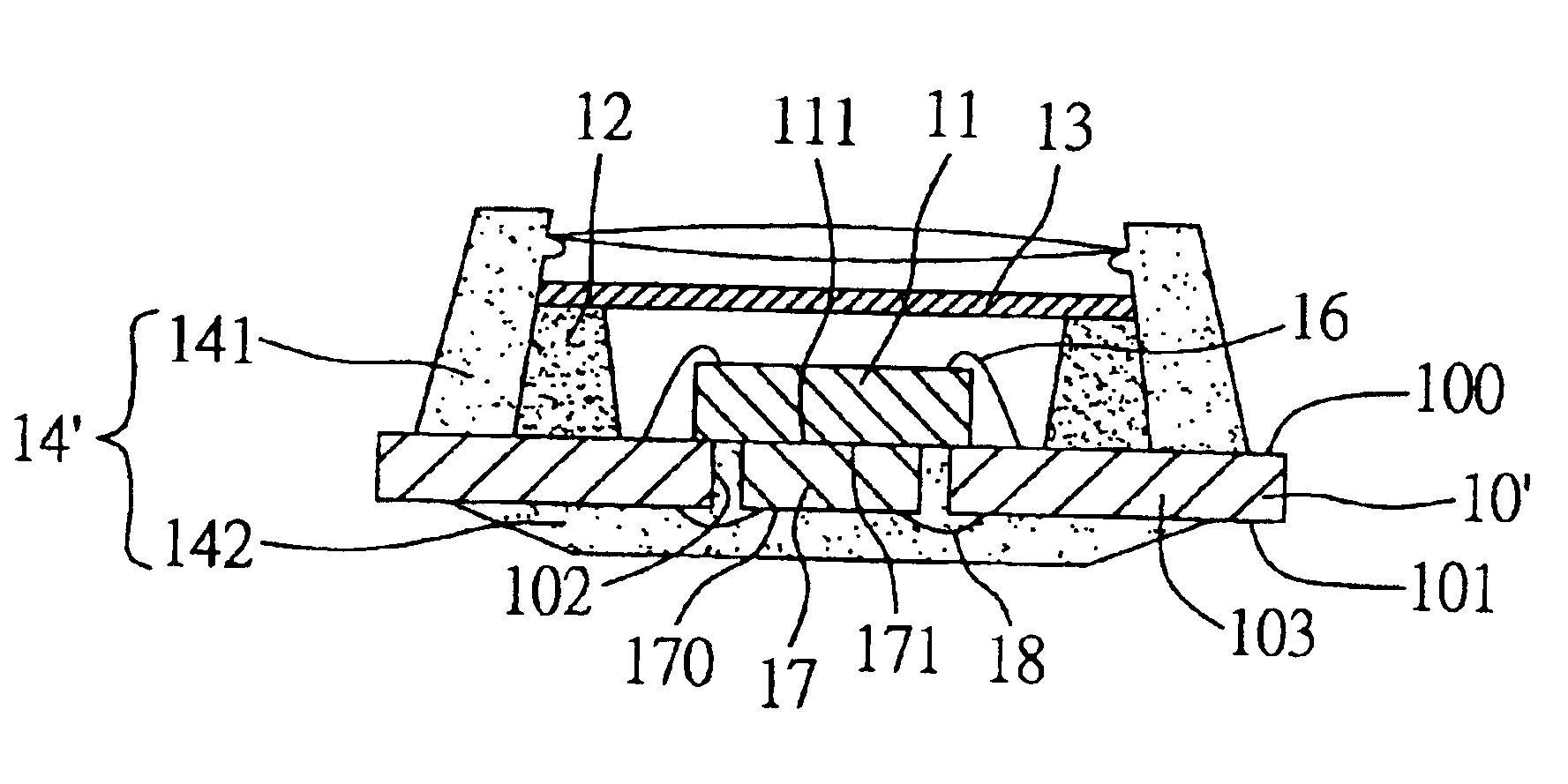
second preferred embodiment
FIG. 3 illustrates a semiconductor package according to a second preferred embodiment of the invention. As shown in FIG. 3 this semiconductor package is structurally similar to that of the above first embodiment but differs in that a chip carrier 10′ is formed with a through hole 102 penetrating through the upper and lower surfaces 100, 101 of the chip carrier 10′, allowing the chip 11 (hereinafter referred to as “first chip”) to be mounted over the through hole 102 on the upper surface 100 of the chip carrier 10′, with the inactive surface 111 of the first chip 11 being partly exposed to the through hole 102. The chip carrier 10′ can be a substrate formed with the through hole 102, or a lead frame having a plurality of leads 103 surrounding the through hole 102. At least one second chip 17 is attached to the first chip 11 via the through hole 102 and received in the through hole 102 of the chip carrier 10′. The second chip 17 has an active surface 170 and an opposite inactive surfa...
PUM
 Abstract
Description
Claims
Application Information