Flip chip on glass sensor package

a technology of glass sensor and flip chip, which is applied in the field of electronic components packaging, can solve the problems of defective operation or failure large volume of image sensor assembly, and large volume of cavity, so as to minimize the volume of cavity, minimize the amount of moisture trapped inside the cavity, and minimize the effect of volum

Inactive Publication Date: 2005-02-01
AMKOR TECH SINGAPORE HLDG PTE LTD
View PDF33 Cites 65 Cited by
  • Summary
  • Abstract
  • Description
  • Claims
  • Application Information

AI Technical Summary

Benefits of technology

The window has an area less than an area of the front surface of the image sensor. Advantageously, this allows the image sensor package to be the size of the image sensor, i.e., the image sensor package is chip size. Further, by avoiding the use of the housing of a prior art image sensor assembly, the image sensor package in accordance with the present invention can also be made relatively thin. Accordingly, the image sensor package is extremely well suited for use with miniature lightweight electronic devices, which require small, thin and lightweight image sensor assemblies.
The window, a bead between the window and the image sensor, and the image sensor define a sealed cavity in which the active area is located. Advantageously, the volume of the cavity is relatively small. By minimizing the volume of the cavity, the amount of any moisture trapped within the cavit...

Problems solved by technology

Disadvantageously, the conventional image sensor assembly described above required a housing to support the window and to seal the image sensor.
However, this housing was relatively bulky and extended upwards from the printed circuit mother board a significant distance, e.g., 0.100 inches (2.54 mm) to 0.120 inches (3.05 mm) or more.
As a result, the image sensor assembly was relatively large.
In the event that moisture was trapped inside of the housing, defective...

Method used


Image

  • Flip chip on glass sensor package
  • Flip chip on glass sensor package
  • Flip chip on glass sensor package

Examples


Embodiment Construction

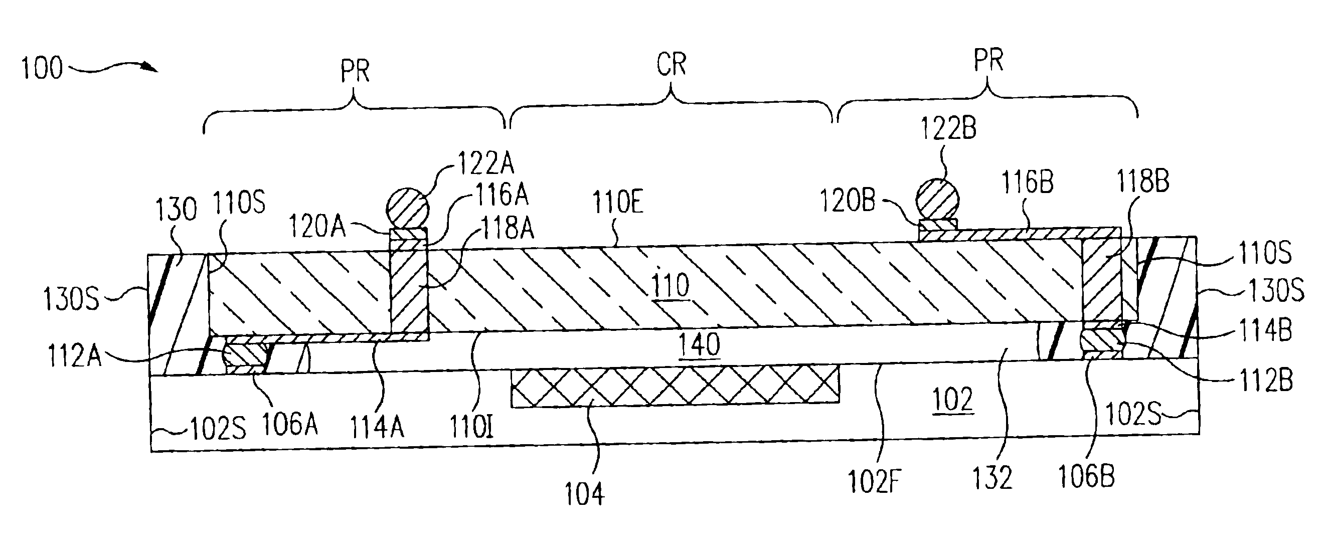
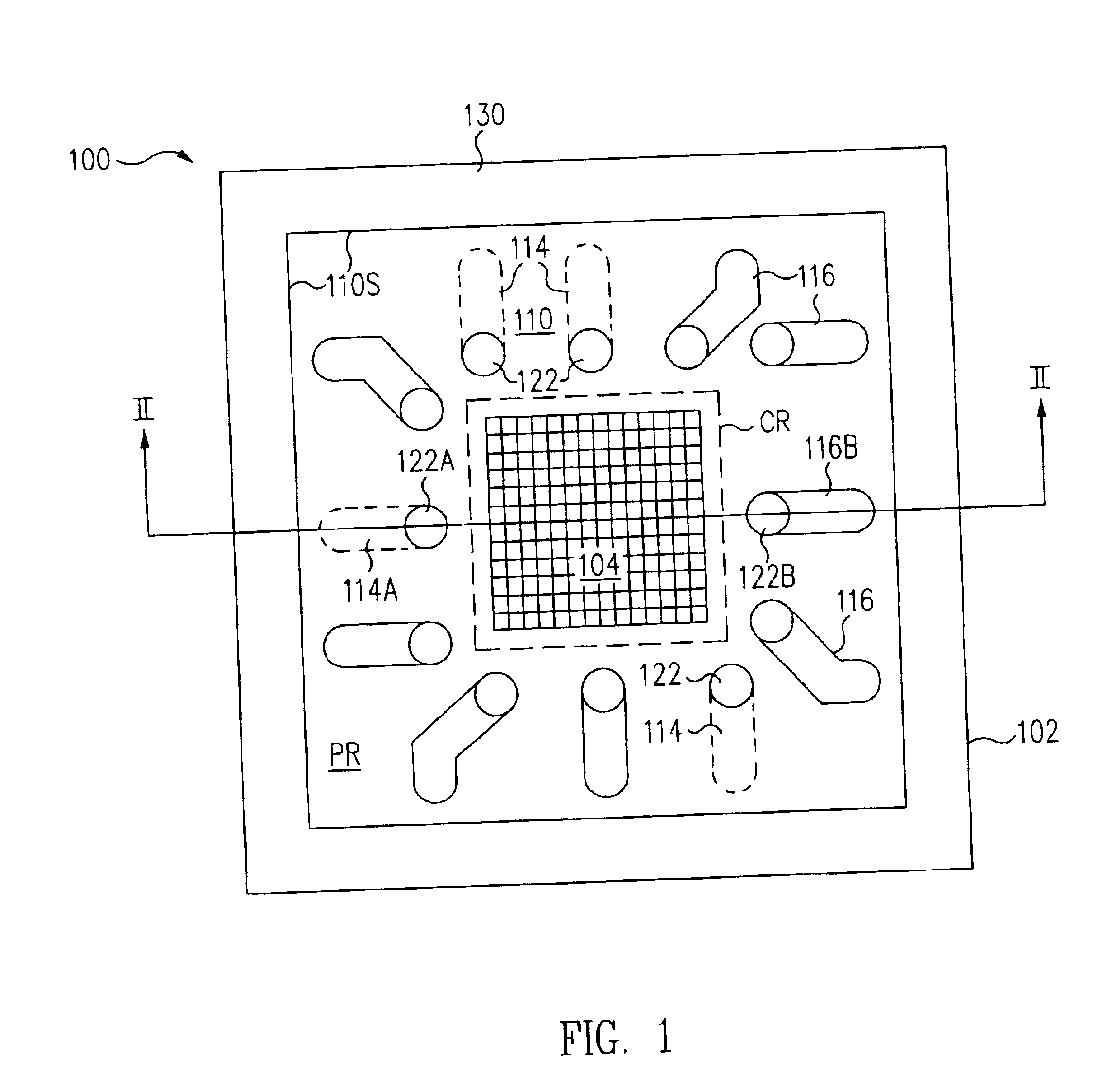
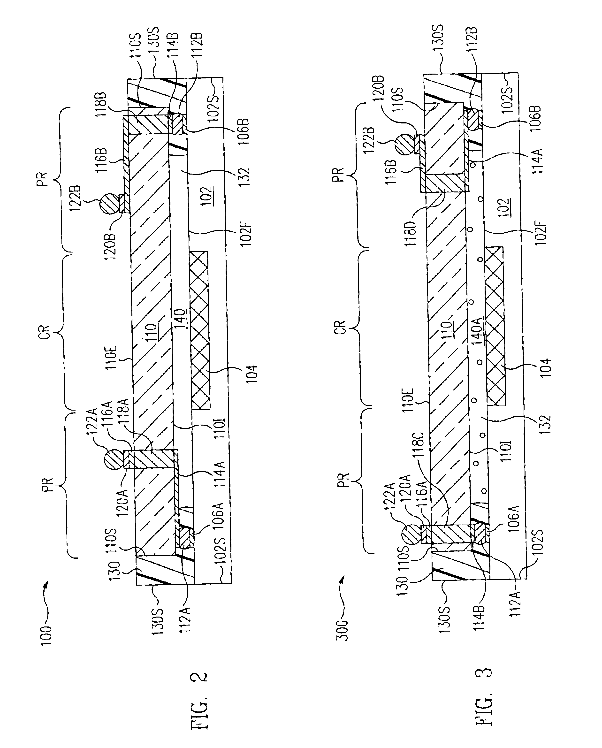
An image sensor package 100 (FIGS. 1, 2) includes an image sensor 102, sometimes called an optical sensor, having an active area 104 and bond pads 106 on a front surface 102F of image sensor 102. A window 110 of image sensor package 100 has an interior surface 110I and an exterior surface 110E opposite interior surface 110I. Electrically conductive interior traces 114 are formed on interior surface 110I of window 110. Window 110 is mounted to image sensor 102 by flip chip bumps 112 formed between bond pads 106 of image sensor 102 and interior traces 114 on interior surface 110I of window 110.

Window 110 includes a central region CR aligned with active area 104 of image sensor 102. A peripheral region PR of window 110 includes interior traces 114, exterior traces 116 formed on exterior surface 110E of window 110, and vias 118 electrically connecting exterior traces 116 to interior traces 114. Pads 120 are formed on exterior traces 116. Interconnection balls 122 are formed on pads 122....


PUM


Abstract

An image sensor package includes an image sensor having an active area and bond pads on a front surface of the image sensor. A window is mounted to the image sensor by flip chip bumps formed between the bond pads of the image sensor and interior traces on an interior surface of the window. The window has an area less than an area of the front surface of the image sensor. A bead is formed between the window and the front surface of the image sensor thus forming a sealed cavity in which the active area is located. The bead has sides coplanar with sides of the image sensor such that the image sensor package is chip size.

Description

BACKGROUND OF THE INVENTION1. Field of the InventionThe present invention relates generally to the packaging of electronic components. More particularly, the present invention relates to an image sensor package.2. Description of the Related ArtImage sensors are well known to those of skill in the art. An image sensor included an active area, which was responsive to electromagnetic radiation. The image sensor was used to fabricate an image sensor assembly.In one prior art image sensor assembly, the image sensor was located within a housing, which supported a window. Radiation passed through the window and struck the active area of the image sensor, which responded to the radiation.To form the image sensor assembly, the image sensor was mounted to a printed circuit mother board. After the image sensor was mounted, a housing was mounted around the image sensor and to the print circuit mother board. This housing provided a seal around the image sensor, while at the same time, supported ...

Claims


Application Information

Patent Timeline
IPC IPC(8): H01L23/02H01L31/0203H01L31/00H01L27/146H04N5/225
CPCH01L27/14618H04N5/2253H01L31/0203H01L2924/0002H04N23/54H01L2924/00
Inventor GLENN, THOMAS P.WEBSTER, STEVENHOLLAWAY, ROY DALE
Owner AMKOR TECH SINGAPORE HLDG PTE LTD
Why Eureka
Try Eureka