

IC package substrate with over voltage protection function
a technology of over voltage protection and substrate, which is applied in the direction of fixed capacitor dielectric, fixed capacitor details, fixed capacitors, etc., can solve the problems of high design cost, limited space, and inability to recover damage to the ic devi
- Summary
- Abstract
- Description
- Claims
- Application Information
AI Technical Summary
Benefits of technology
Problems solved by technology
Method used
Image

Examples
Embodiment Construction
The embodiments of the present invention are described with reference to the drawings. The same elements in the drawing have the same reference numerals.
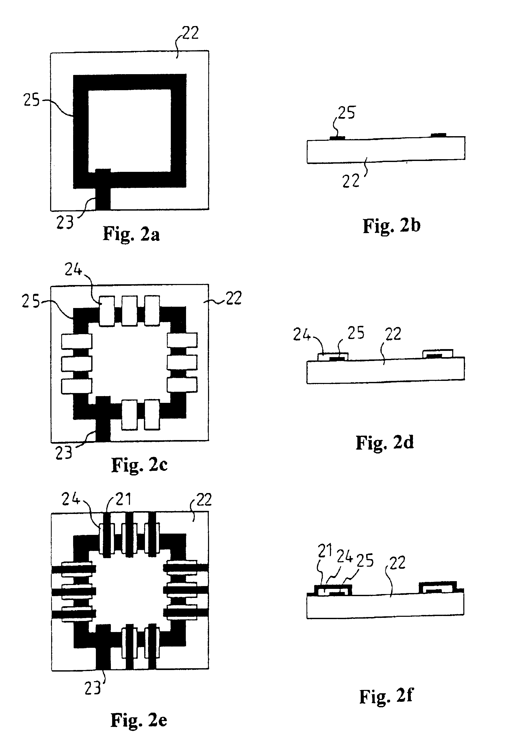
In FIGS. 2a and 2b, a lower electrode (25) is disposed on a substrate (22), wherein a grounding line (23) and the lower electrode (25) are connected. In another embodiment, the grounding line and the lower electrode can be separated.
In FIGS. 2c and 2d, protection material layers (24) are disposed on the lower electrodes (25). In FIGS. 2e and 2f, one or more upper electrodes (21) are disposed on the protection material layers (24), wherein the protection material layers are variable resistance material layers.
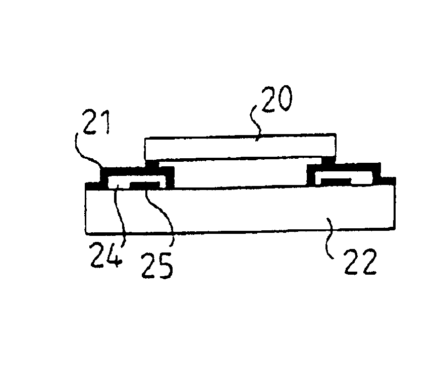
In FIGS. 2g and 2h, an IC chip (20) is installed on the substrate. The IC chip is a flip chip, and is connected with the upper electrodes (21) and the grounding line (23) by soldering. In another embodiment of the present invention, the chip (20) is connected with the upper electrodes (21) and the grounding line (23) by wire bon...
PUM
 Abstract
Description
Claims
Application Information