Array substrate for liquid crystal display device

a liquid crystal display and array substrate technology, applied in static indicating devices, instruments, optics, etc., can solve the problems of deterioration of the transmissivity of the lcd, poor image quality of the lcd, and lc molecules are hardly arranged properly, so as to enhance the reliability of the lcd

Inactive Publication Date: 2005-02-01
LG DISPLAY CO LTD
View PDF4 Cites 13 Cited by
  • Summary
  • Abstract
  • Description
  • Claims
  • Application Information

AI Technical Summary

Benefits of technology

One object of the present invention is to provide an array substrate for a falling time delay caused in a gate pulse due to RC delay.
Another object of the present invention is to provide an array substrate for enhancing reliability of an LCD.

Problems solved by technology

In particular, when the falling time of the gate pulse G(N) is prolonged, the image quality of the LCD worsens.
As a result, the LC molecules are hardly arranged properly.
Moreover, the transmissivity of the LCD deteriorates.
Additionally, the picture displayed may be blurred, or there may be an afterimage and flickering.
These phenomena adversely affect the quality of the LCD.
However, these conventional methods increase LCD costs and do not completely solve the various problems caused by RC delay.

Method used


Image

  • Array substrate for liquid crystal display device
  • Array substrate for liquid crystal display device
  • Array substrate for liquid crystal display device

Examples


Embodiment Construction

Reference will now be made in detail to the illustrated embodiment of the present invention, which is illustrated in the accompanying drawings. Wherever possible, the similar reference numbers will be used throughout the drawings to refer to the same or like parts.

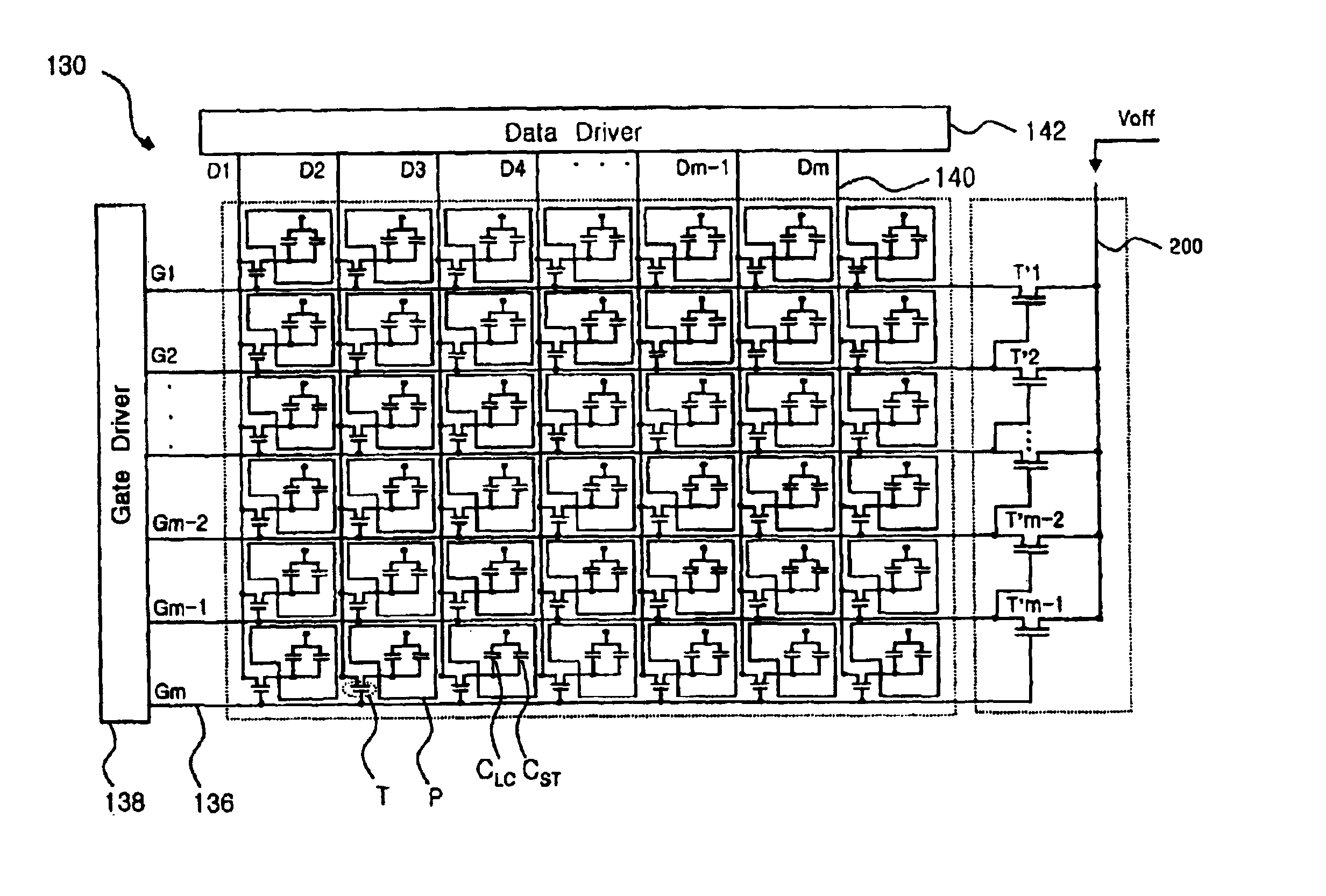
FIG. 5 is a cross-sectional view of a pixel of an LCD panel according to the present invention. FIG. 6 is a schematic diagram showing a main component of an active matrix LCD according to the present invention.

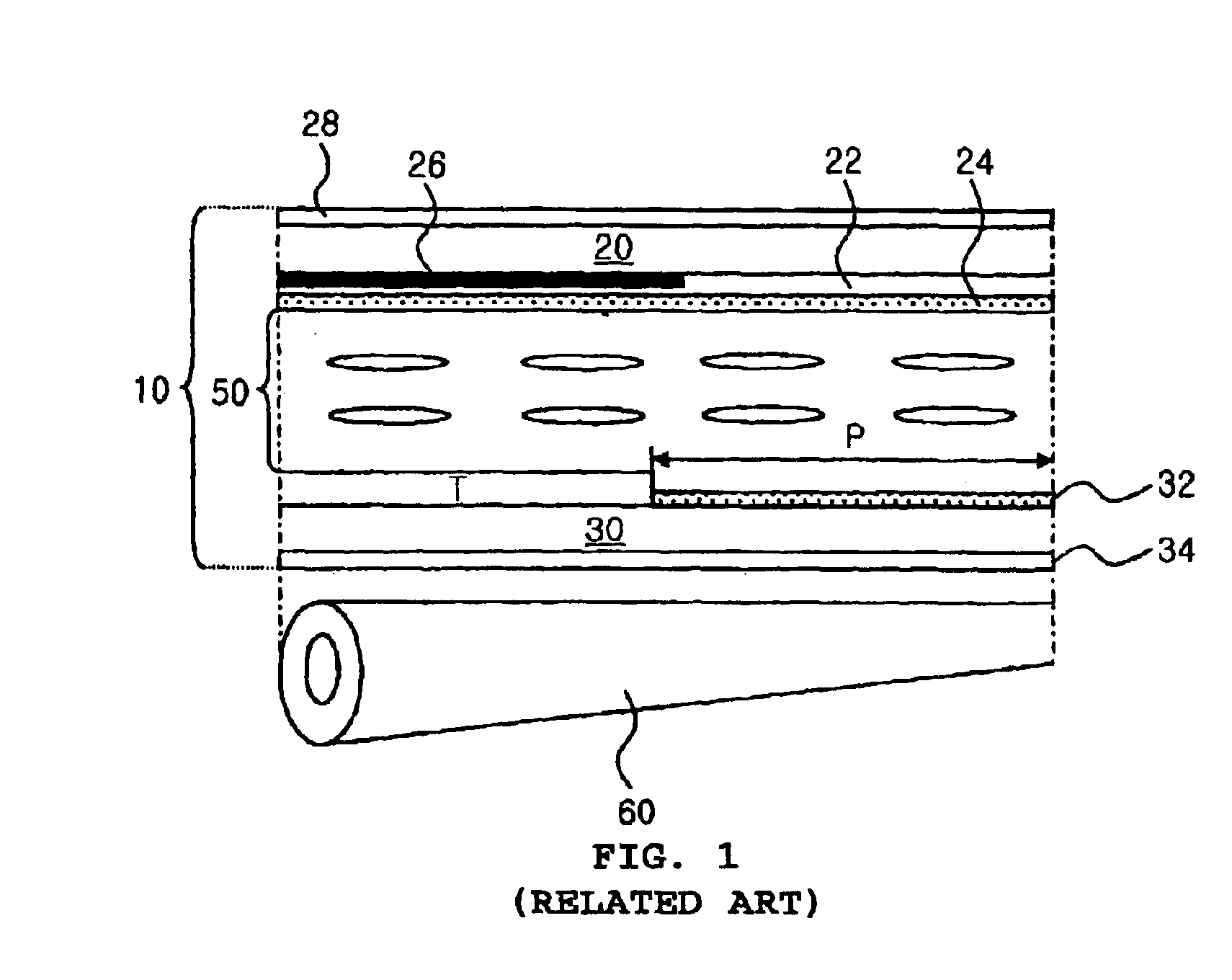
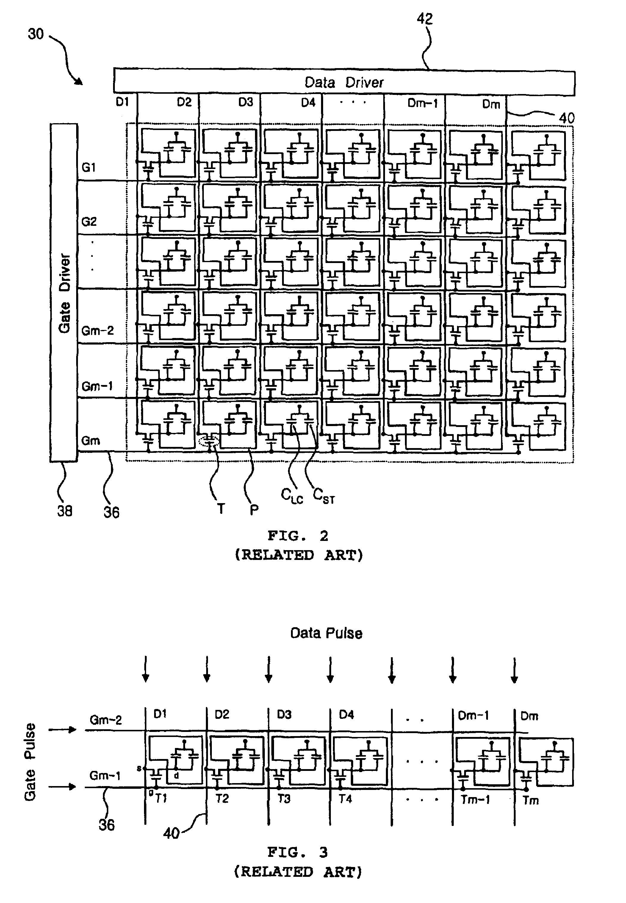
As shown in FIGS. 5 and 6, the LCD panel 110 of the present invention includes an upper color filter substrate 120, a lower array substrate 130 and an LC interposed between the upper color filter substrate 120 and the lower array substrate 130. In the upper color filter substrate 120, a color filter layer 122 is disposed on a rear surface of a transparent substrate 1, and a common electrode 124 applying an electrode field to the liquid crystal is disposed on the color filter layer 122. The color filter layer 122 can ...


PUM

PropertyMeasurementUnit
transparentaaaaaaaaaa
OFF voltageaaaaaaaaaa
ground voltageaaaaaaaaaa

Abstract

The present invention is related to an array substrate for use in a liquid crystal display. The array substrate includes a transparent substrate; a plurality of gate lines arranged over the transparent substrate in a transverse direction; a plurality of data lines arranged over the transparent substrate in a longitudinal direction substantially perpendicular to the plurality of gate lines, intersections of the plurality of data lines and the plurality of gate lines defining a plurality of pixel regions; a gate driver contacting ends of the plurality of gate lines and sequentially scanning a gate pulse to the plurality of gate lines; a data driver contacting ends of the plurality of data lines and applying a data pulse to the plurality of data lines; a plurality of pixel electrodes disposed in the plurality of pixel regions; a plurality of first thin-film transistors disposed in the plurality of pixel regions, each first thin-film transistor including a gate electrode connected to a gate line, a source electrode connected to a data line, and a drain electrode connected to the pixel region; a feed line outputting an OFF voltage to the plurality of first thin-film transistors; and a plurality of second thin-film transistors contacting each other and connecting the feed line to the plurality of gate lines.

Description

BACKGROUND OF THE INVENTION1. Field of the InventionThe present invention relates in general to a liquid crystal display device and, more particularly, to an array substrate having a plurality of thin-film transistors that compensates for a falling time delay caused by an RC delay of a gate pulse.2. Discussion of the Related ArtUntil recently, a cathode-ray tube (CRT) has generally been used for display systems. However, use of flat panel displays is increasingly common, because of their small depth, desirably low weight, and relatively minimal power consumption. Presently, thin-film transistor-liquid crystal displays (TFT-LCDs) are being developed with high resolution and small depth.Liquid crystal display (LCD) devices generally make use of optical anisotropy and polarization properties of liquid crystal molecules to control alignment orientation. The alignment direction of the liquid crystal molecules can be controlled by application of an electrical field. Accordingly, when an e...

Claims


Application Information

Patent Timeline
Patent Type & Authority Patents(United States)
IPC IPC(8): G02F1/13G02F1/136H01L21/00G09G3/36
CPCG09G3/3648G09G3/3677G09G2320/0223G09G2310/0251G09G2320/0209G09G2300/0408G02F1/136
Inventor LEE, JU-YOUNG
Owner LG DISPLAY CO LTD
Why Eureka
Try Eureka