Electronic memory circuit and related manufacturing method

a technology of electronic memory and manufacturing method, applied in the field of electronic memory circuits, can solve the problems of non-uniform implanted region, difficult to remove, and the current in the common source region will reach relatively high values

Inactive Publication Date: 2005-02-08
STMICROELECTRONICS SRL
View PDF13 Cites 6 Cited by
  • Summary
  • Abstract
  • Description
  • Claims
  • Application Information

AI Technical Summary

Problems solved by technology

In the portion of the source region common to two bytes, wherein the first layer of polysilicon has been removed during the first step of definition of the floating gates, the second step of removal of the first layer of polysilicon for defining the final gate region is not selective enough for discriminating the first layer of polysilicon or the surface of the substrate of silicon in single-crystal form.
First of all, these notches may become receptacles for contaminating material, which would be hard to remove because of the small dimensions of the notches 30 themselves.
Further, because of the differences in height present on the surface of the source region, the subsequent implantation of dopant provides non-uniform implanted region.
This drawback is particularly significant for the EEPROM parallel access memory matrices, because all the cells of the same byte will be read at the same time and thus the current in the common source region will reach relatively high values.
This may lead to a read error on the single memory cell because of the resistance introduced by the presence of these notches.

Method used


Image

  • Electronic memory circuit and related manufacturing method
  • Electronic memory circuit and related manufacturing method
  • Electronic memory circuit and related manufacturing method

Examples


Embodiment Construction

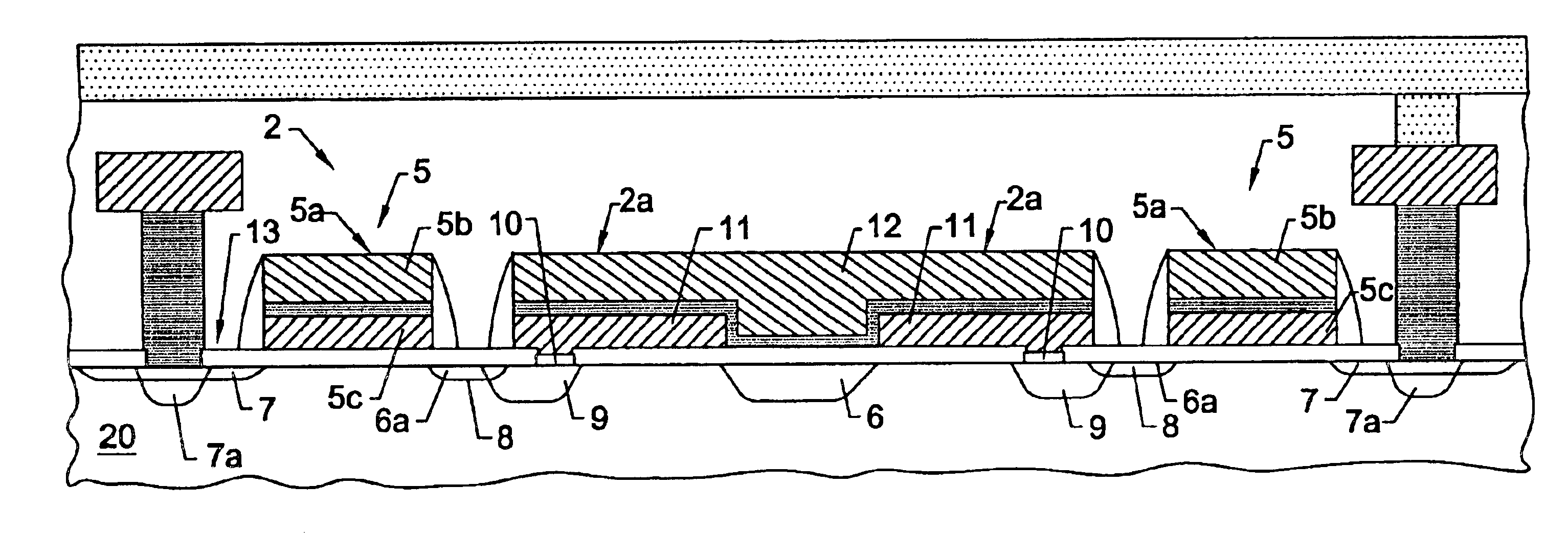
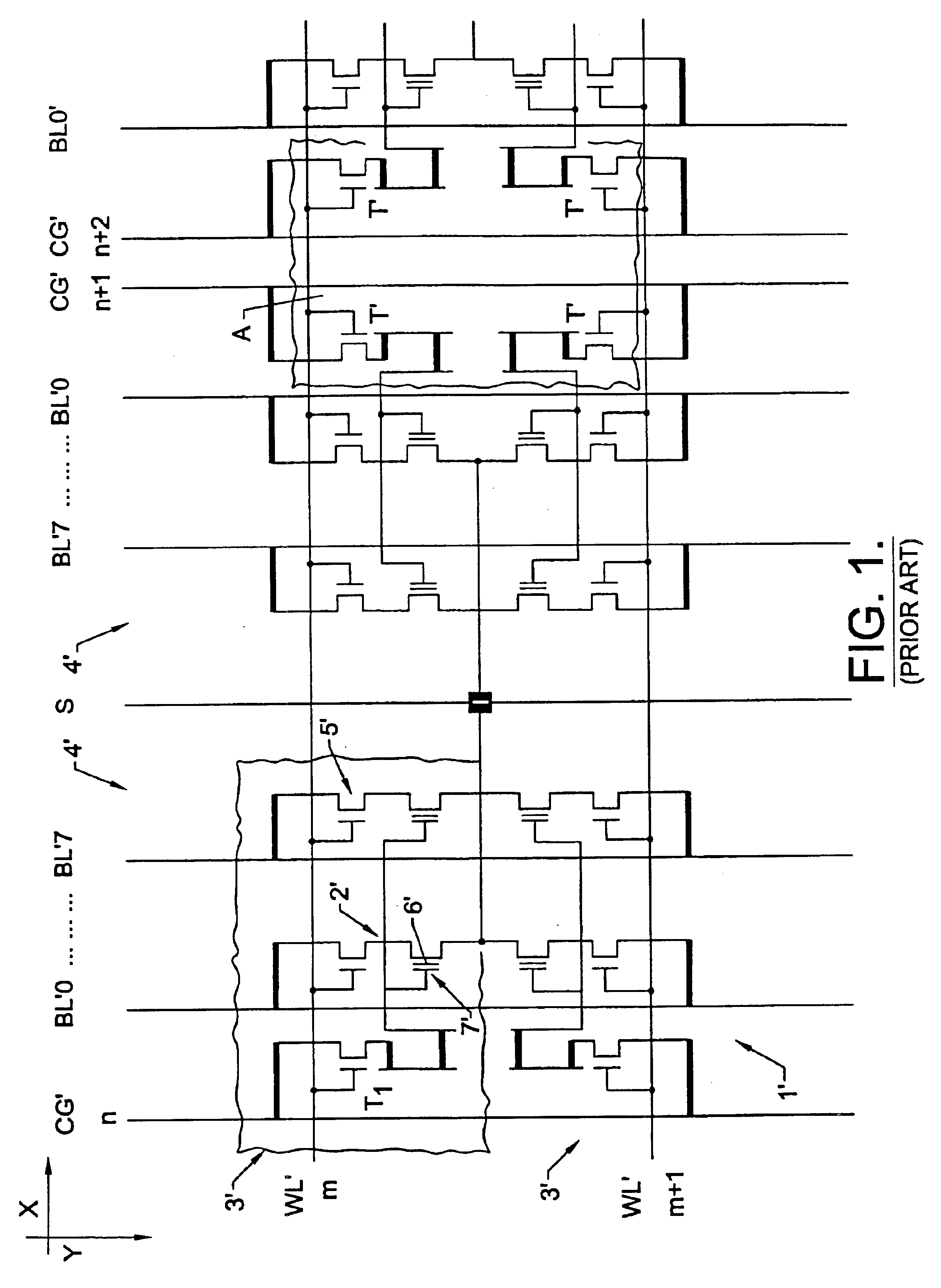
With reference to the drawings, an electronic memory circuit 1 including a matrix of EEPROM memory cells 2 will now be described. The structure 1 is realized as a semiconductor integrated circuit, incorporating, for example, thousands of cells 2. In FIG. 6 only a portion of such circuit is indicated. The matrix according to the invention includes a plurality of rows 3, comprising the word lines WL1, WLm and a plurality of columns 4 comprising bit lines of the matrix.

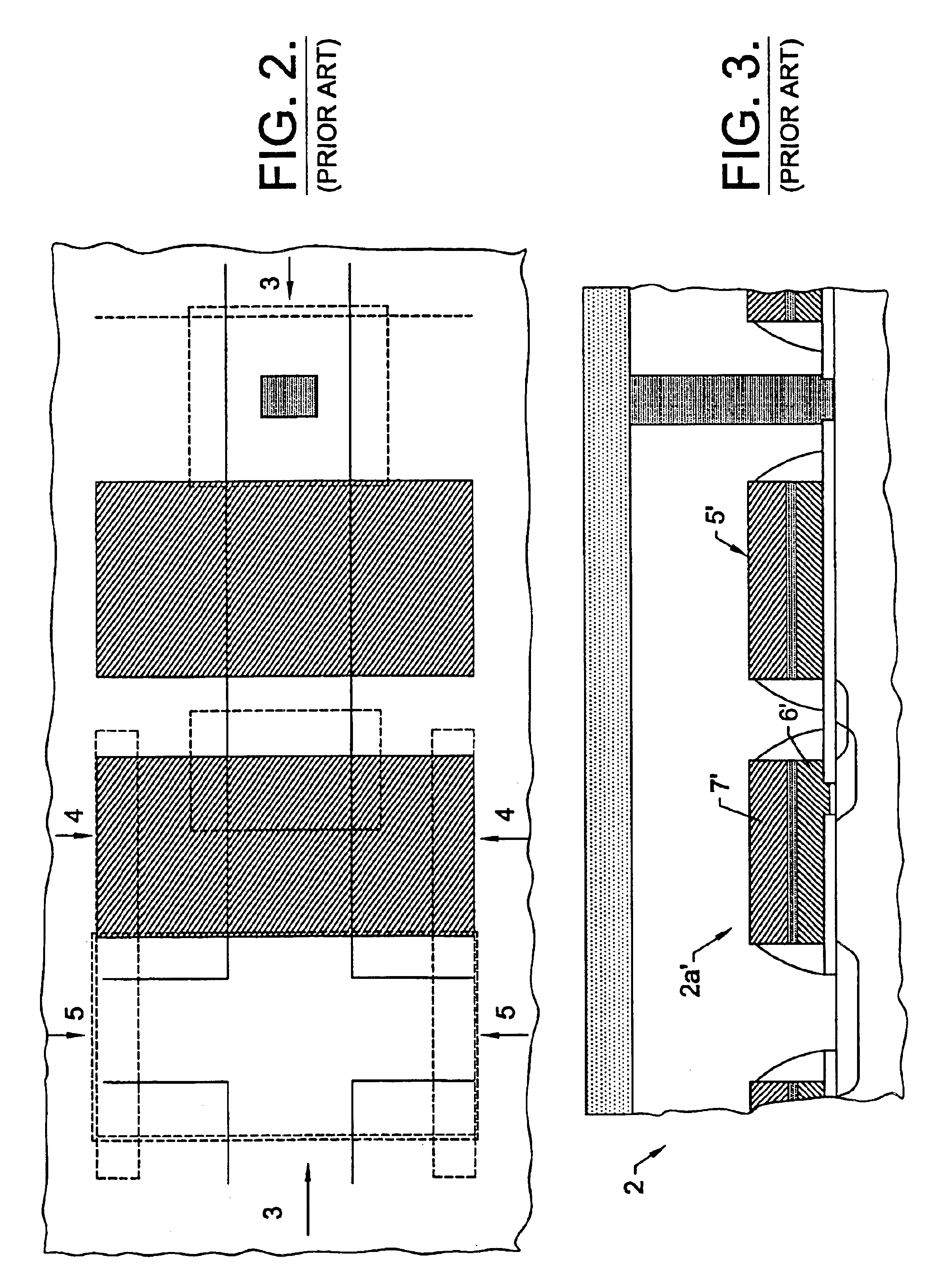
The columns 4 also comprise control gate lines CG. Groups of eight lines of bit, BL0, BL1 . . . BL7 are grouped in a byte 9a. For each byte 9a, a memory cell 2 is connected to each bit line Bli. Each EEPROM cell 2 comprises a MOS transistor 2a connected in series to a selection transistor 5, as would readily be appreciated by those skilled in the art. In particular each selection transistor comprises a source region 6a and a drain region 7 of N-type formed in a substrate 20 of P-type.

As is typical, such region 7 also com...


PUM


Abstract

An electronic memory circuit comprises a matrix of EEPROM memory cells. Each memory cell includes a MOS floating gate transistor and a selection transistor. The matrix includes a plurality of rows and columns, with each row being provided with a word line and each column comprising a bit line organized in line groups so as to group the matrix cells in bytes, each of which has an associated control gate line. A pair of cells have a common source region, and each cell symmetrically provided with respect to this common source region has a common control gate region.

Description

FIELD OF THE INVENTIONThe present invention relates to circuits, and, more particularly, to an electronic memory circuit.BACKGROUND OF THE INVENTIONAs known, EEPROM memories, while being a non-volatile type of memory, allow electrical modification of the information contained therein in either a write or an erase step. It is also known that each EEPROM cell comprises a floating gate transistor and a selection transistor. Once the selection transistor is enabled, it is possible to alter the state of the associated floating gate transistor, by exploiting a passage of electrons for tunnel effect through a thin layer of silicon oxide, the so-called tunnel oxide. Such a thin layer is provided below a portion of the floating gate region of the floating gate transistor, in which the charge is stored.During the write and erase steps of the cells, positive voltages are usually applied to the diffusion below the tunnel region or to the control gate. Such voltages are between 8 and 18 Volts in...

Claims


Application Information

Patent Timeline
Patent Type & Authority Patents(United States)
IPC IPC(8): G11C16/04H01L27/115H01L21/70H01L21/8247
CPCG11C16/0433H01L27/11524H01L27/11521H01L27/115H10B41/35H10B69/00H10B41/30
Inventor PIO, FEDERICO
Owner STMICROELECTRONICS SRL
Why Eureka
Try Eureka