Printed circuit board and soldering structure for electronic parts thereto

a printed circuit board and electronic part technology, applied in the direction of metal working apparatus, manufacturing tools, soldering apparatus, etc., can solve the problems of affecting the quality of printed circuit boards, parts shaken loose from printed circuit patterns, tedious and time-consuming work, etc., to prevent thermal energy from leaking outwards.

Inactive Publication Date: 2005-02-08
ORION ELECTRIC CO LTD
View PDF7 Cites 17 Cited by
  • Summary
  • Abstract
  • Description
  • Claims
  • Application Information

AI Technical Summary

Benefits of technology

To attain these objects a printed circuit board including a substrate having circuit patterns printed on first and second surfaces thereof is improved according to the present invention in that it has a plurality of composite lands each comprising a first land having a terminal hole made at its center for inserting the terminal of a selected electric or electronic part or device, and a plurality of second lands each being contiguous to and extending outwards from the first land, and that, for each of the composite lands, thermal insulating areas are provided radially outwardly of the first lands and circumferentially between adjacents ones of the second lands, the thermal insulating areas being constituted by areas of the substrate devoid of a conductive layer, such as copper foil, so as to expose the substrate surface of the printed circuit board. The exposed areas effectively prevent thermal energy from leaking outwards from the composite land when soldering an electric or electronic part or device to the composite land.
The soldering structure according to the present invention has substrate-exposed zones having no thermally conductive foils contiguous to the first and second lands, thus preventing leakage of thermal energy from the first and second lands. Thus, sufficient quantities of thermal energy can be confined to the limited area to assure reliable soldering. Still advantageously, the ridged cone-like shape is useful in building up the solder lump to be sufficiently strong to assure that the terminal of the part or device is fixedly gripped; the terminal can be fixedly supported by the surrounding cone-like solder lump and ridge lumps as a whole. This soldering structure requires a minimum quantity of solder material.

Problems solved by technology

Accordingly the cone-like solder lump 55 can hardly provide a holding strength sufficient to assure that the electric or electronic part is fixedly held on the printed circuit pattern.
As a matter of fact, when electric or electronic devices having such printed circuit boards are transported, some parts are shaken loose from their printed circuit patterns.
This, however, is tedious and time-consuming work.
Also, it may be possible that an additional quantity of solder will cause short-circuiting.
Division of the land into separate sections proposed in JP2000-91737(A) is not so effective in confining the thermal energy to the limited area for soldering, and hence, in increasing the solder quantities in joining the terminal and the land.

Method used


Image

  • Printed circuit board and soldering structure for electronic parts thereto
  • Printed circuit board and soldering structure for electronic parts thereto
  • Printed circuit board and soldering structure for electronic parts thereto

Examples


Embodiment Construction

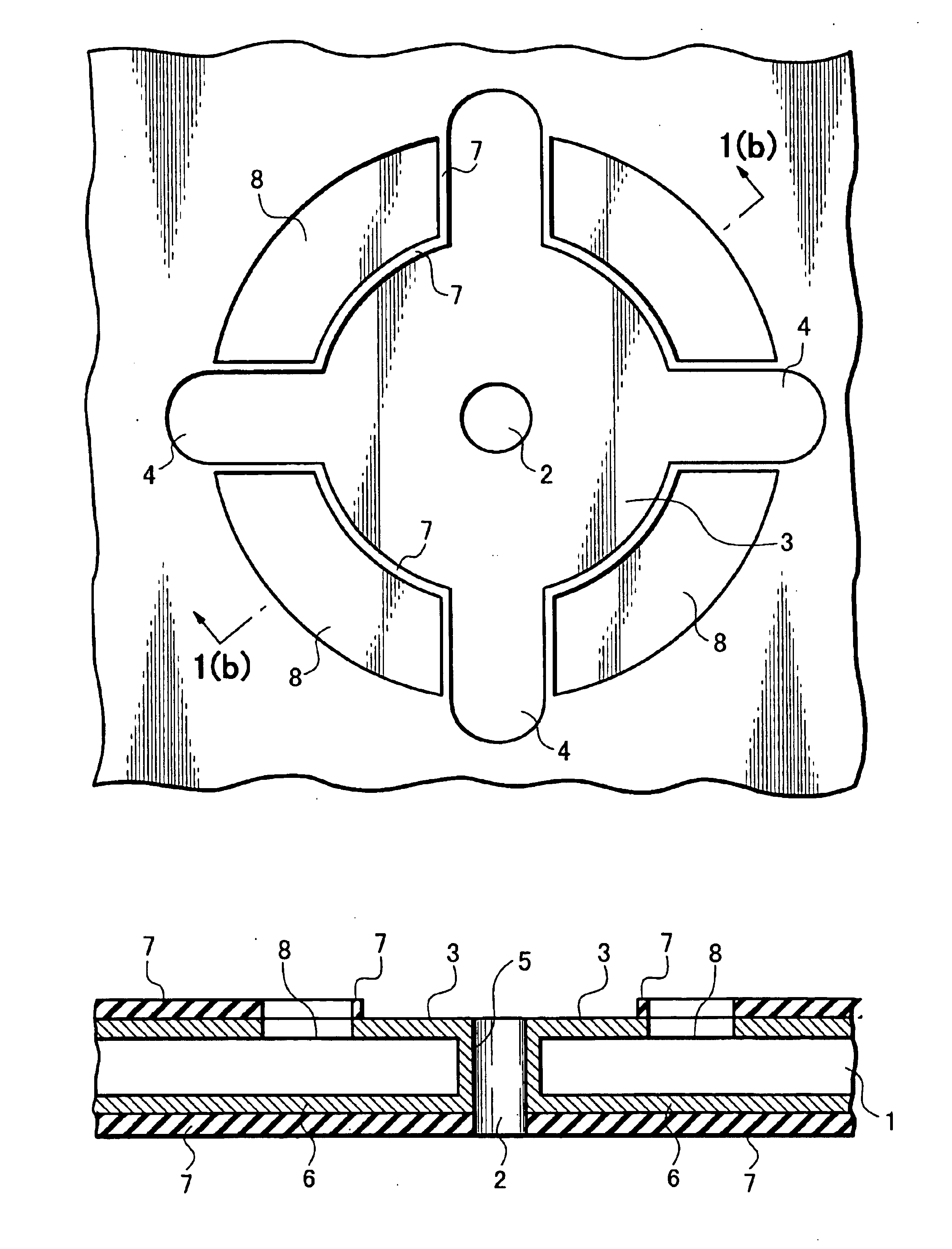
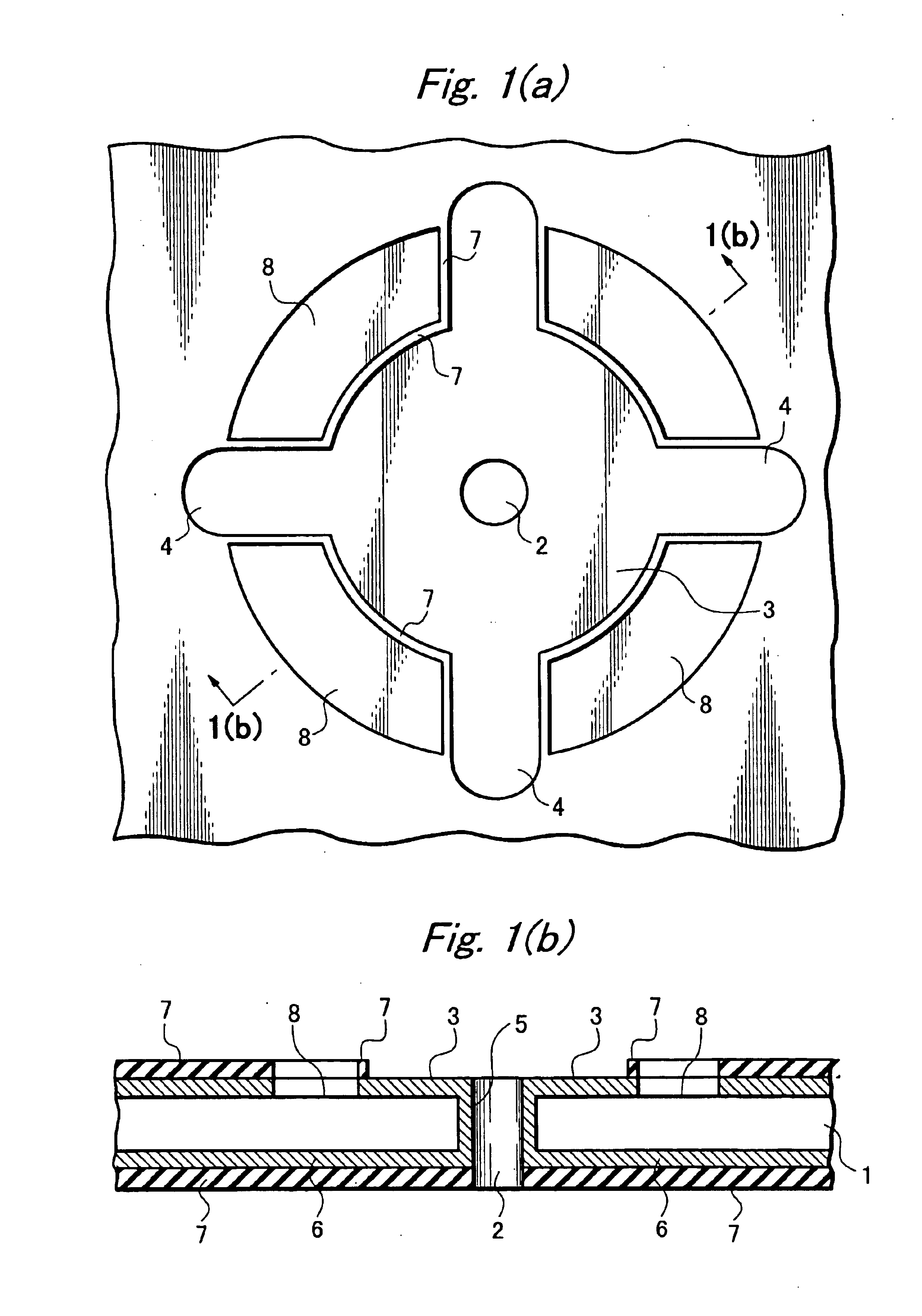
Referring to FIGS. 1(a) and 1(b), a printed circuit board has circuit patterns printed on its substrate 1. As shown, a first circular land 3 has a through hole 2 to insert the terminal of a selected electric or electronic part or device, and four second radial lands 4 are contiguous to the first circular land 3, extending outwards therefrom. The substrate 1 has circuit patterns 6 printed on its opposite sides, and electric or electronic parts or devices are mounted and joined to the composite lands with their terminals inserted in the terminal holes 2 and soldered to the composite lands.

The composite land of copper foil is connected to the underlying circuit pattern 6 on the rear side via the conductor layer 5, which is applied to the inner circumference of the terminal hole 2, as seen from FIG. 1(b). A selected part or device is mounted on the rear side of the substrate 1 with its terminal inserted into the terminal hole 2.

As seen from FIG. 1(a), the surface of the printed circuit ...


PUM

PropertyMeasurementUnit
electricallyaaaaaaaaaa
electrically conductiveaaaaaaaaaa
areaaaaaaaaaaa

Abstract

A printed circuit board having circuit patterns printed thereon has a plurality of composite lands each including a first land having a terminal hole formed at its center for inserting the terminal of a selected electric or electronic part or device, and a plurality of second lands each being contiguous to and extending outwards from the first land. The areas contiguous to the contours of the first and second lands have no conductive foils, such as copper foils, thereon such that the substrate surface of the printed circuit board is exposed in these areas. The exposed areas are effective to confine the thermal energy in the limited areas for soldering. And the composite land shape defines a ridged cone-like solder lump, which can fixedly grip the terminal of the part or device.

Description

BACKGROUND OF THE INVENTION1. Field of the InventionThe present invention relates to a printed circuit board having electric or electronic parts soldered to its circuit patterns.2. Related ArtElectric or electronic apparatuses use printed circuit boards, which have a variety of electric or electronic parts soldered to their circuit patterns. Specifically such circuit patterns are formed by labyrinth-like copper foils and the like, each having electric or electronic parts soldered to lands with their terminals inserted in the terminal holes, which are made in the lands.FIG. 5(a) is a plan view of a land 51 whereas FIG. 5(b) is a sectional view of a land 51, showing a terminal 54 of a selected electric or electronic part soldered to the land 51. The land 51 is formed on the rear side (the upper side in FIG. 5(b) of a substrate 50, and the land 51 has a terminal hole 52 formed at its center. The land 51 is surrounded by a resist layer 53 of an insulating synthetic resin to prevent sold...

Claims


Application Information

Patent Timeline
Patent Type & Authority Patents(United States)
IPC IPC(8): B23K1/00H05K3/34H05K1/02H05K1/11
CPCB23K1/0016H05K1/0201H05K1/116H05K3/3447B23K2201/42H05K2201/0989H05K3/3452H05K2201/062H05K2201/09381H05K2201/0969B23K2101/42
Inventor MIYAJIMA, YOSHIYUKI
Owner ORION ELECTRIC CO LTD
Why Eureka
Try Eureka