Defect inspection apparatus and defect inspection method

a technology of defect inspection and inspection apparatus, which is applied in the direction of material analysis using wave/particle radiation, semiconductor/solid-state device testing/measurement, instruments, etc., can solve the problems of requiring at least several days for collecting the x-ray spectra of all defects due to edx, and analyzing a defective portion using edx requires a long tim

Inactive Publication Date: 2005-02-15
HITACHI LTD
View PDF11 Cites 26 Cited by
  • Summary
  • Abstract
  • Description
  • Claims
  • Application Information

AI Technical Summary

Problems solved by technology

Analysis of a defective portion using EDX requires a long time.
Specifically, the time required for collecting data on one point is much longer than the time required for the foreign particle inspection apparatus or the defective reviewing device.
The collecting the X-ray spectra of all defects due

Method used


Image

  • Defect inspection apparatus and defect inspection method
  • Defect inspection apparatus and defect inspection method
  • Defect inspection apparatus and defect inspection method

Examples


second embodiment

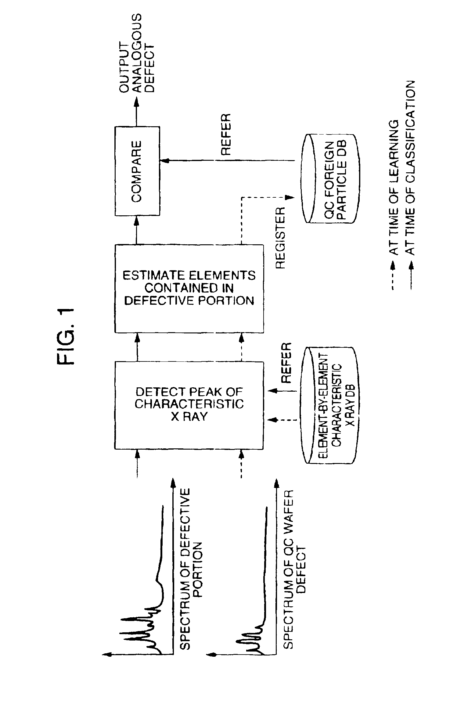
Now, a second embodiment of the invention will be explained. According to the invention, defects are classified and the cause of the defects estimated by EDX or by using both EDX and the image at the same time. The second embodiment described below has a similar hardware configuration to the first embodiment but is different from the first embodiment in the method of processing the detection signal and the configuration of the data base. In the second embodiment of the invention, the foreign particle information unique to the fabrication system having a dummy wafer (face plate wafer) for system management are collected and registered as reference information for defect classification.

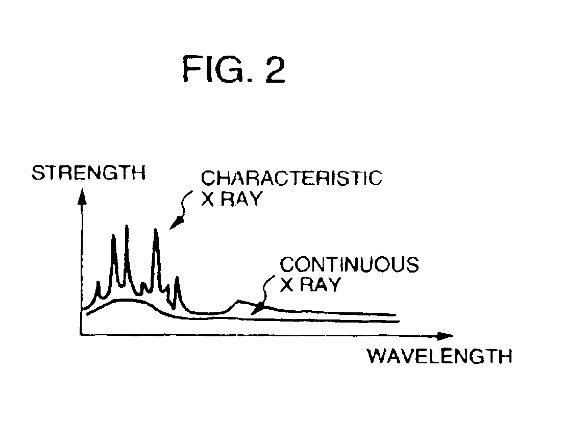
FIG. 1 is a flowchart for explaining the operation of processing the detection signal according to the second embodiment of the invention. With reference to FIG. 1, the processing operation will be briefly explained. The process is configured of two stages including learning and classification.

(Learning...


PUM


Abstract

An apparatus and a method for automatically inspecting a defect by an electron beam using an X-ray detector. The composition of a defective portion is analyzed with higher rapidity and the cause of the defect is easily and accurately determined based on an X-ray spectrum. The X-ray spectrum and the image of foreign particles formed on a process QC wafer are registered as reference data, and the defects generated on a process wafer are classified by collation with the reference data. The use of both the X-ray spectrum and the detected image optimizes the operating conditions for X-ray detection. A defect of which the X ray is to be detected is selected based on the result of classification of defect images automatically collected, and the defect is classified according to the features including both the composition and the external appearance.

Description

BACKGROUND OF THE INVENTIONThe present invention relates to a defect inspection apparatus and a defect inspection method, or in particular to a defect inspection apparatus and a defect inspection method using a technique suitable for inspection and analysis of a defect generated on a semiconductor wafer in the process of fabricating a semiconductor electronic circuit, in which an electron beam is radiated on a defective portion and the X-ray spectrum generated is analyzed.(1) Outline of Defect Analysis by EDXA method called EDX (Energy Dispersion X-ray Spectrum) is known as a conventional technique for analyzing the cause of the foreign particles generated on a semiconductor wafer during the semiconductor fabrication process. In this EDX method, an electron beam is radiated on a defect on a semiconductor wafer, and the energy dispersion (spectrum) of the X ray generated from a defective portion and the neighborhood thereof is analyzed to estimate the element composition of the forei...

Claims


Application Information

Patent Timeline
IPC IPC(8): G01N23/225G01N23/22G06T1/00H01L21/66
CPCG06T7/0004G01N23/225
Inventor OKUDA, HIROHITOTAKAGI, YUJIHONDA, TOSHIFUMI
Owner HITACHI LTD
Why Eureka
Try Eureka