High-breakdown-voltage semiconductor device

a semiconductor device, high-breakdown technology, applied in the direction of semiconductor devices, electrical apparatus, transistors, etc., can solve the problems of difficult deepening the gate region, resist also easily remaining outside the trench, electric short circuit or deterioration of the flatness of the element surface,

Inactive Publication Date: 2005-02-15
KK TOSHIBA
View PDF1 Cites 53 Cited by
  • Summary
  • Abstract
  • Description
  • Claims
  • Application Information

AI Technical Summary

Problems solved by technology

Moreover, it is very difficult to deepen the gate region because of a small diffusion coefficient of impurities in SiC.
However, when the resist is allowed to reflow in the above-described method, there is a problem that the resist also easily remains outside the trench.
In this case, when a pattern of the resist generated by the reflow is used as the mask to etch the surface, the metal film also remains outside the trench, and electric short-circuit or deterioration of flatness of the element surface is caused.
There is a problem that manufacturing yield is deteriorated and element properties are also deteriorated.
On the other hand, for a switch-off property of a SIT, in the element in which the metal film is selectively left in contact with the bottom and lower side surface of the trench to form the gate electrode, the spread of the depletion layer in the width direction of the channel cannot be said to be necessarily sufficient.
There is a problem that the switch-off property is not sufficient.
In the element in which a control electrode is formed in the p-type semiconductor layer in the above-described method, it cannot be said that the spread of the depletion layer is sufficient, and there is a problem that the switch-off property is not sufficient.

Method used


Image

  • High-breakdown-voltage semiconductor device
  • High-breakdown-voltage semiconductor device
  • High-breakdown-voltage semiconductor device

Examples


first embodiment

A first embodiment relates to a high-breakdown-voltage semiconductor device (SIT).

First, structural characteristics and effect in the SIT of the present embodiment will be described.

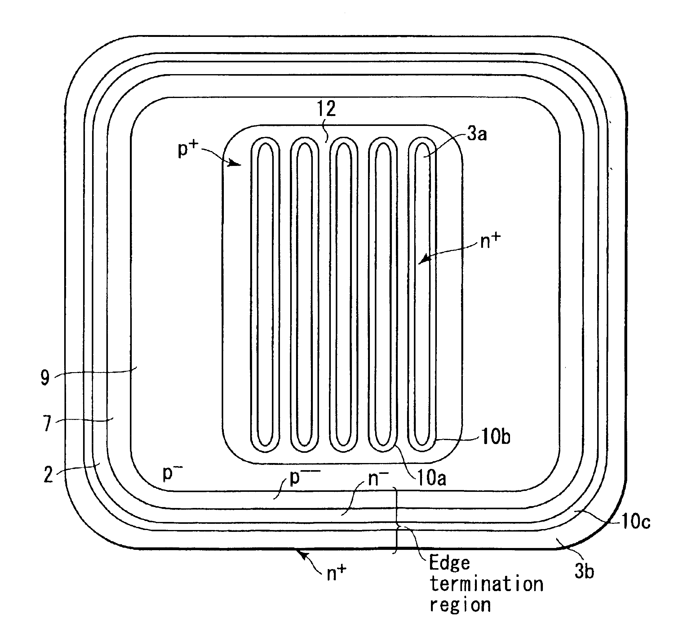
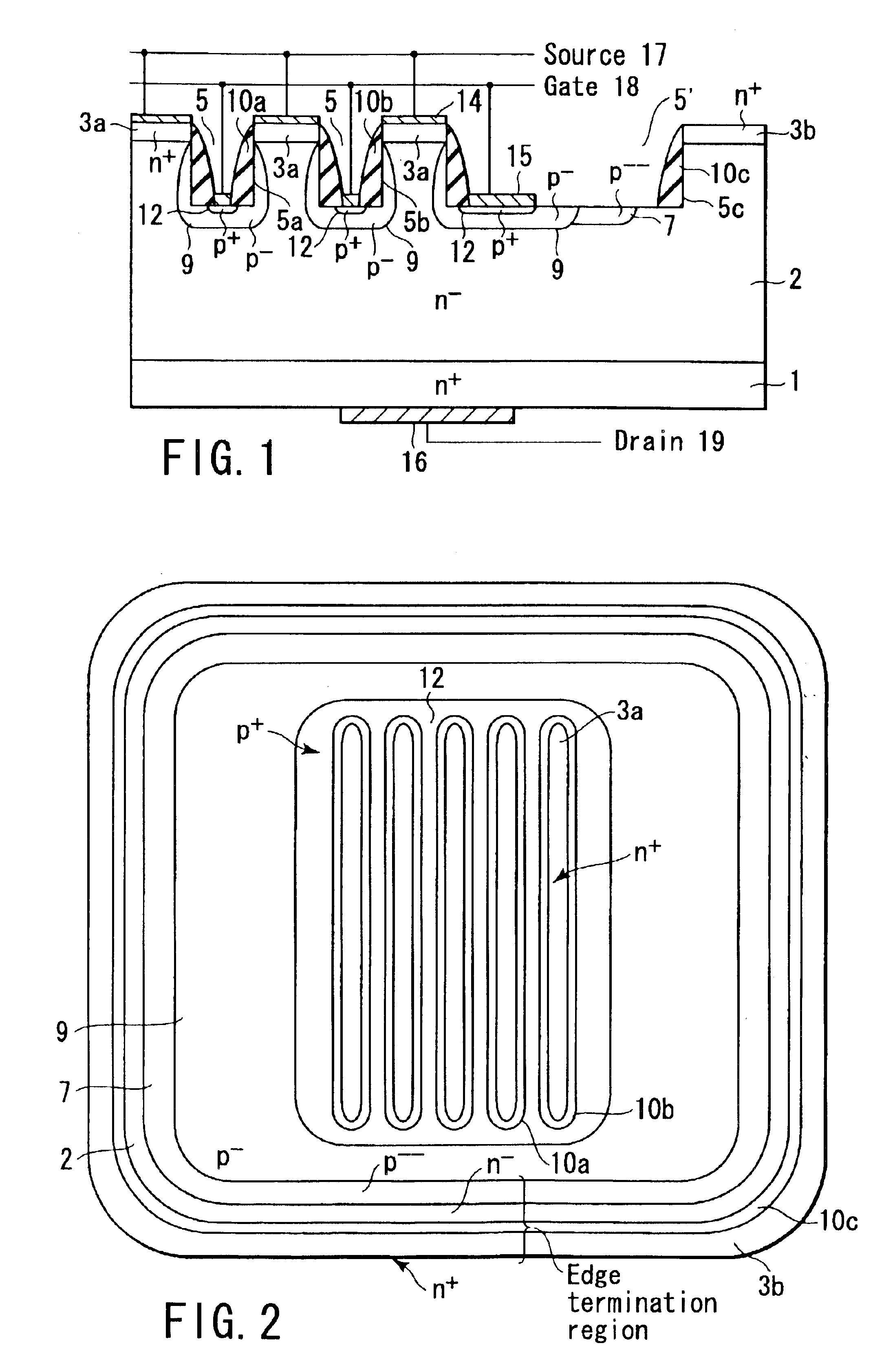
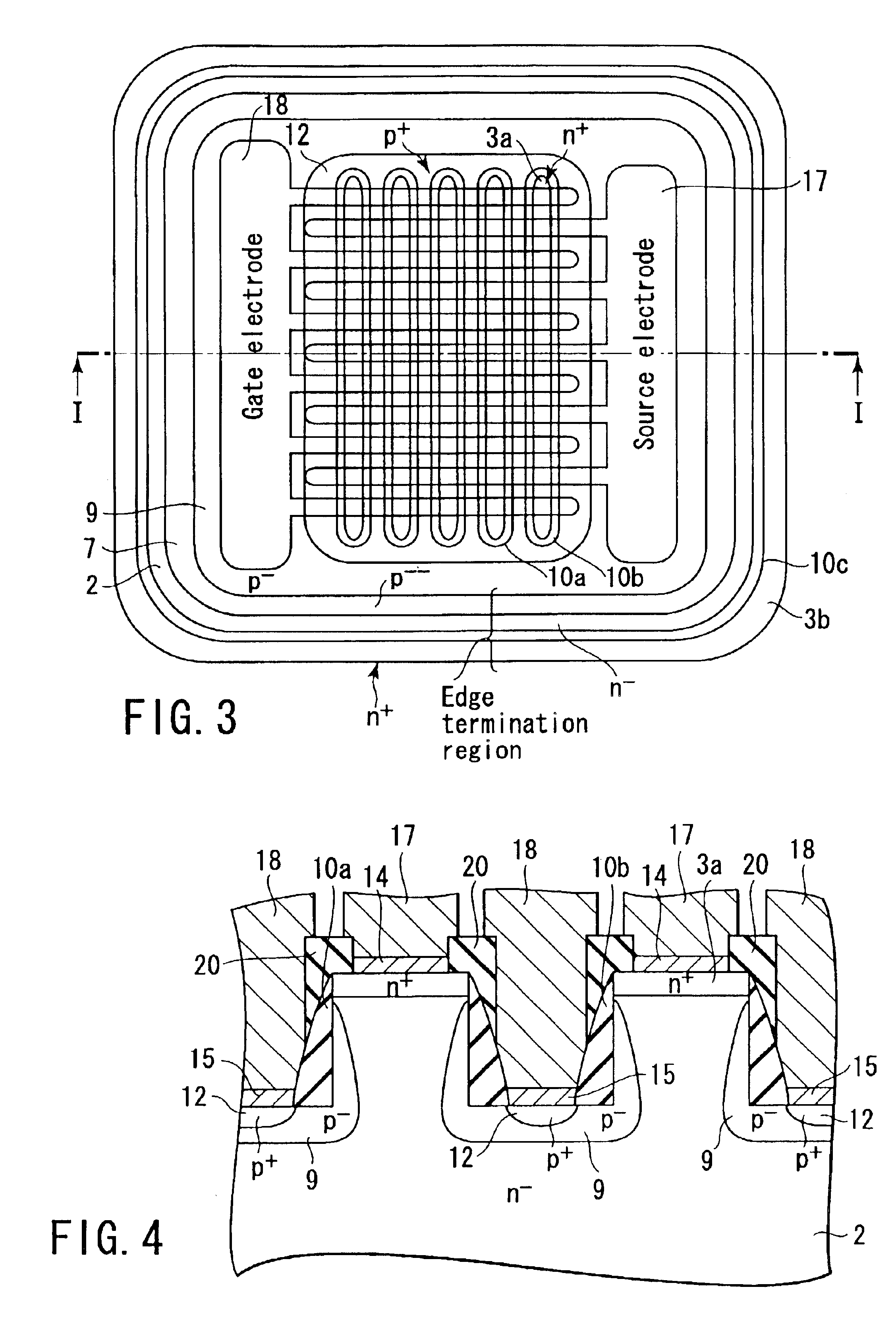
As shown in FIG. 1, in one surface of an n-type high-resistance semiconductor layer (SiC layer), an n-type first semiconductor region (SiC layer) 3a is selectively disposed as a source region which has a resistance lower than that of a high-resistance semiconductor layer 2 (higher impurity concentration). The impurity concentration and thickness of the high-resistance semiconductor layer 2 are determined by a designed breakdown voltage. For example, the impurity concentration is in a range of 1×10¹⁴ to 1×1016 cm−3 and the thickness is in a range of 5 to 100 μm. The source region 3a has an impurity concentration, for example, of 1×1020 cm−3. Examples of an n-type dopant for use include nitrogen, phosphor, and arsenic.

As shown in FIGS. 1 to 3, trench portions 5 and 5′ are disposed in the high-resistance se...

second embodiment

FIG. 13 is a sectional view of the high-breakdown-voltage semiconductor device (SI thyristor) according to a second embodiment of the present invention. An n+ layer on the back surface in the first embodiment (FIG. 1) is changed to a p+ layer, and the static induction (SI) thyristor can be formed. Since the configuration is similar to that of the first embodiment, the same components are denoted with the same reference numerals, and redundant description is omitted. Moreover, a top plan view is the same as FIG. 2, and is therefore omitted.

First, the structural characteristics and effect in the SI thyristor of the present embodiment will be described. As shown in FIG. 13, on one surface (back surface) of the n-type high-resistance semiconductor layer (SiC layer) 2, a low-resistance p+-type semiconductor layer 1′ is disposed as a collector layer. Reference numeral 16′ denotes a collector electrode, and 19′ denotes a collector electrode lead wire.

The impurity concentration and thicknes...

third embodiment

The high-breakdown-voltage semiconductor device of a third embodiment relates to a junction barrier Schottky diode (JBS).

First, the structural characteristic and effect in the JBS of the present embodiment will be described. As shown in FIG. 15, on one surface of an n-type high-resistance semiconductor layer (SiC layer) 102, a Schottky electrode 114 is disposed to form Schottky junction with this high-resistance semiconductor layer 102. Reference numeral 103a denotes a Schottky junction region. The impurity concentration and thickness of the high-resistance semiconductor layer 102 are determined by the designed breakdown voltage. For example, the impurity concentration is in a range of 1×10¹⁴ to 1×1016 cm−3 and the thickness is in a range of 5 to 50 μm. Furthermore, when conduction modulation is used, the thickness may also be 100 μm. Examples of the n-type dopant for use include nitrogen, phosphor, and arsenic. Examples of the material of the Schottky electrode 114 for use include ...


PUM


Abstract

A high-breakdown-voltage semiconductor device comprises a high-resistance semiconductor layer, trenches formed on the surface thereof in a longitudinal plane shape and in parallel, first regions formed on the semiconductor layer to be sandwiched between adjacent ones of the trenches and having an impurity concentration higher than that of the semiconductor layer, a second region having opposite conductivity to the first regions and continuously disposed in a trench sidewall and bottom portion, a sidewall insulating film disposed on the second region of the trench sidewall, a third region disposed on the second region of the trench bottom portion and having the same conductivity as and the higher impurity concentration than the second region, a fourth region disposed on the back surface of the semiconductor layer, a first electrode formed on each first region, a second electrode connected to the third region, and a third electrode formed on the fourth region.

Description

BACKGROUND OF THE INVENTION1. Field of the InventionThe present invention relates to a high-breakdown-voltage semiconductor device, particularly to high-breakdown-voltage semiconductor devices such as a power controlling static induction transistor, static induction thyristor, and diode.2. Description of the Related ArtA semiconductor element for power control in which silicon carbide (hereinafter abbreviated as SiC) is used as a wide gap semiconductor material has superior characteristics of high speed and low loss as compared with a related-art element in which silicon is used. There has been a demand for practical use of the semiconductor element. In recent years, a large number of semiconductor elements using SiC, such as a Schottky barrier diode, MOSFET, and static induction transistor (hereinafter abbreviated as SIT) have been presented. It has been confirmed that the properties of the elements are far superior to those of an element using silicon.A structure and manufacturing...

Claims


Application Information

Patent Timeline
Patent Type & Authority Patents(United States)
IPC IPC(8): H01L29/10H01L29/02H01L29/66H01L29/739H01L29/78H01L29/772H01L29/06H01L29/24
CPCH01L29/0615H01L29/0661H01L29/0692H01L29/1095H01L29/872H01L29/7392H01L29/7395H01L29/7722H01L29/7802H01L29/66068H01L29/1608H01L29/7811
Inventor HATAKEYAMA, TETSUOSHINOHE, TAKASHI
Owner KK TOSHIBA
Why Eureka
Try Eureka