

Sensor array and method for detecting the condition of a transistor in a sensor array
a technology of sensor array and array, which is applied in the direction of individual semiconductor device testing, instruments, material analysis, etc., can solve the problems of large reliability problems, the application practicability of the known sensor array, and the observation of reliability problems
- Summary
- Abstract
- Description
- Claims
- Application Information
AI Technical Summary
Benefits of technology
Problems solved by technology
Method used
Image

Examples
Embodiment Construction
Identical elements in the figures are labeled below with the same references.
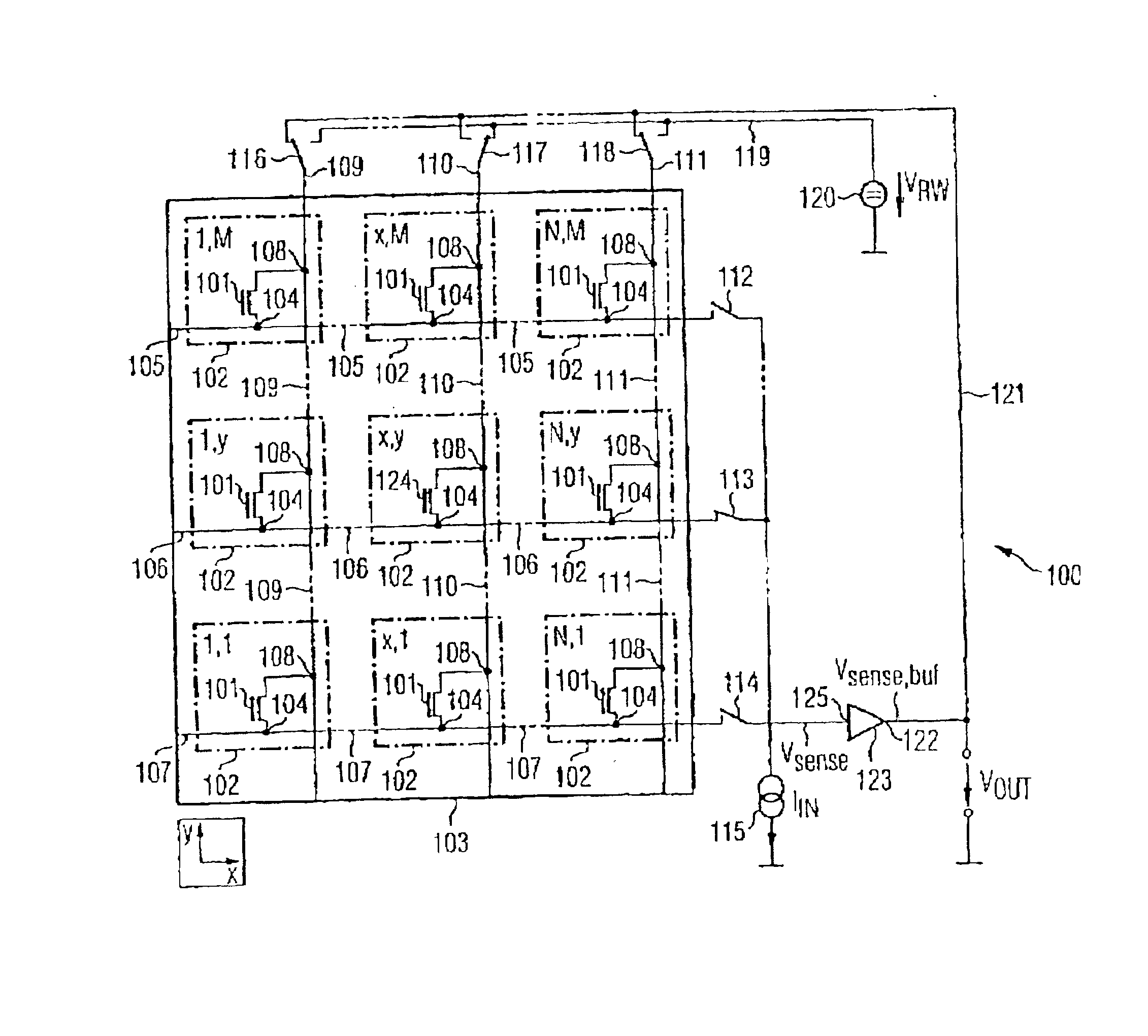
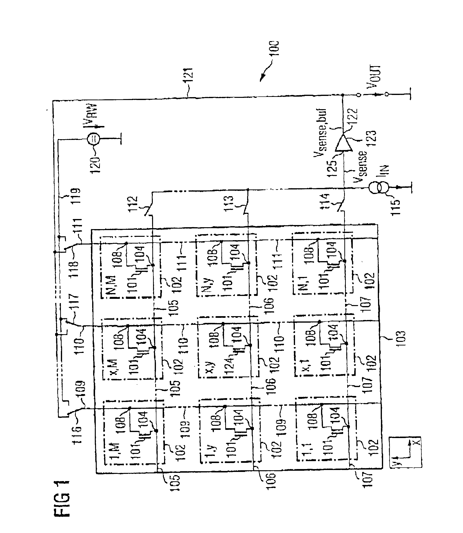
FIG. 1 shows a sensor array 100 according to a first exemplary embodiment of the invention.
The sensor array 100 contains MOS field effect transistors 101 designed as a sensor.
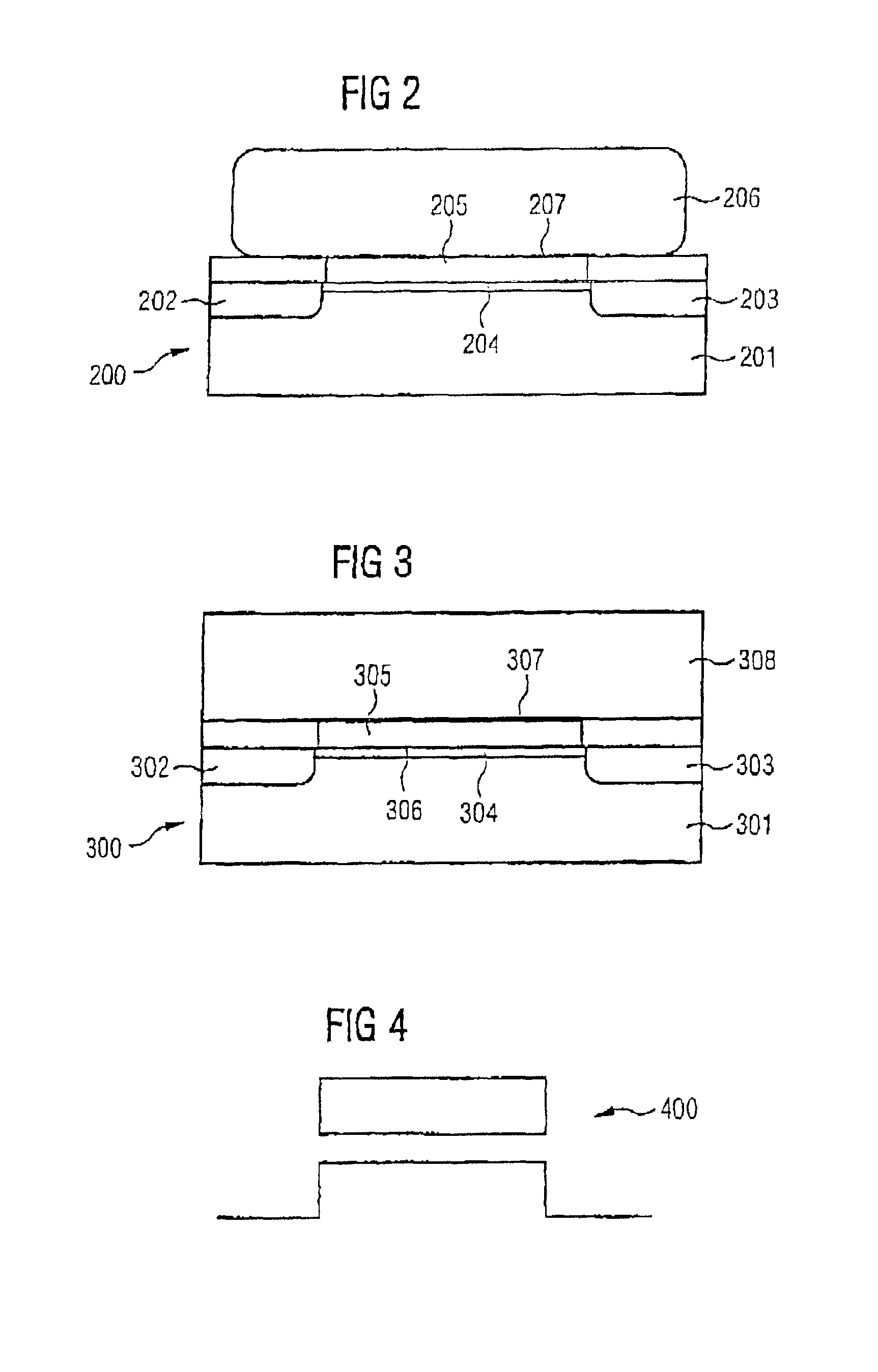
The field effect transistor depicted in FIG. 2 or in FIG. 3 may be used, for instance, as such a field effect transistor.
In addition, the field effect transistors described in [1] and [2] may alternatively be used as sensor in the sensor array 100.
Each field effect transistor 101 forms a sensor cell 102.
The sensor array 100 contains M * N sensor cells 102, the sensor cells 102, and hence the field effect transistors 101, being arranged in N columns and M rows in the form of a matrix 103. This means that the sensor array 100 contains N sensor cells 102 in each row. The sensor array 100 contains M rows, i.e. M sensor cells 102 in each column of the sensor array 100.
FIG. 4 shows the symbol 400 for a field effect transistor 101 as used in ...
PUM
 Abstract
Description
Claims
Application Information