

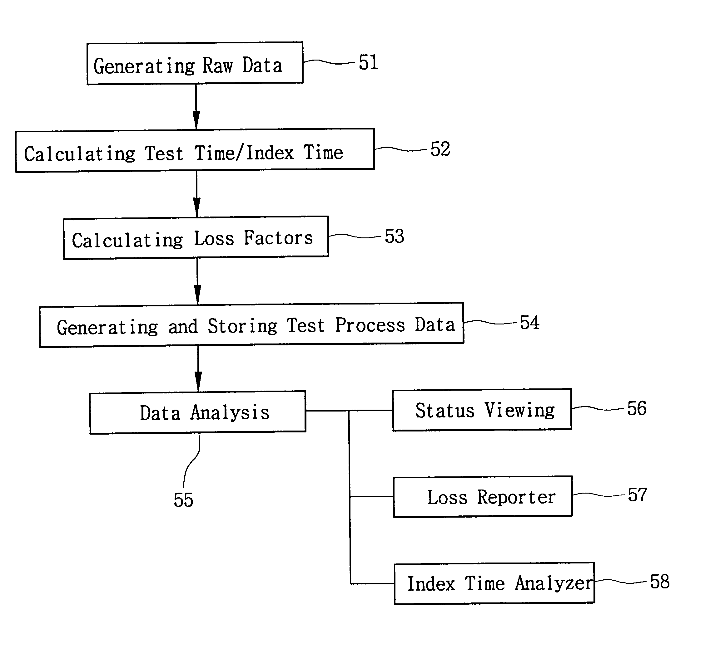
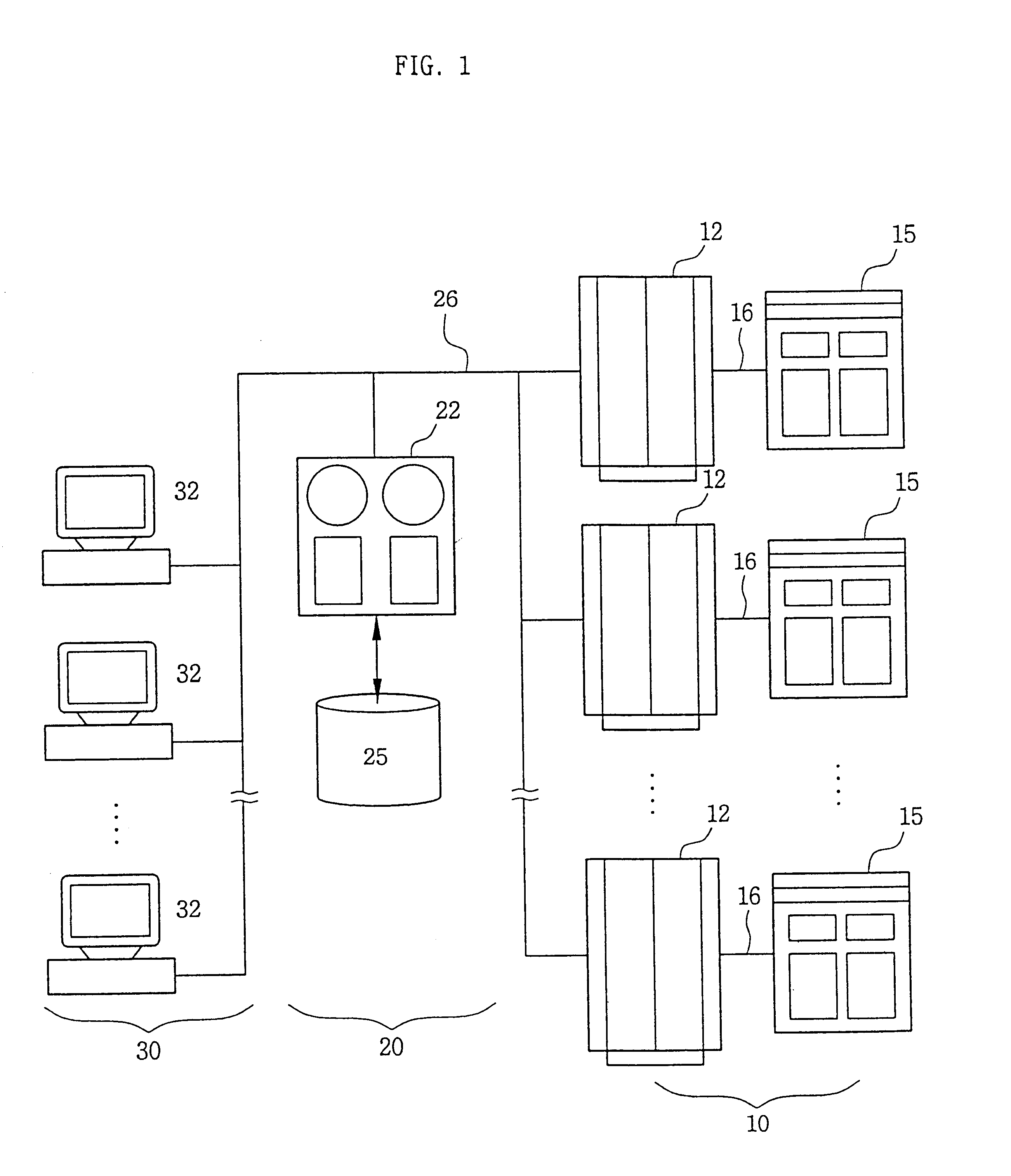
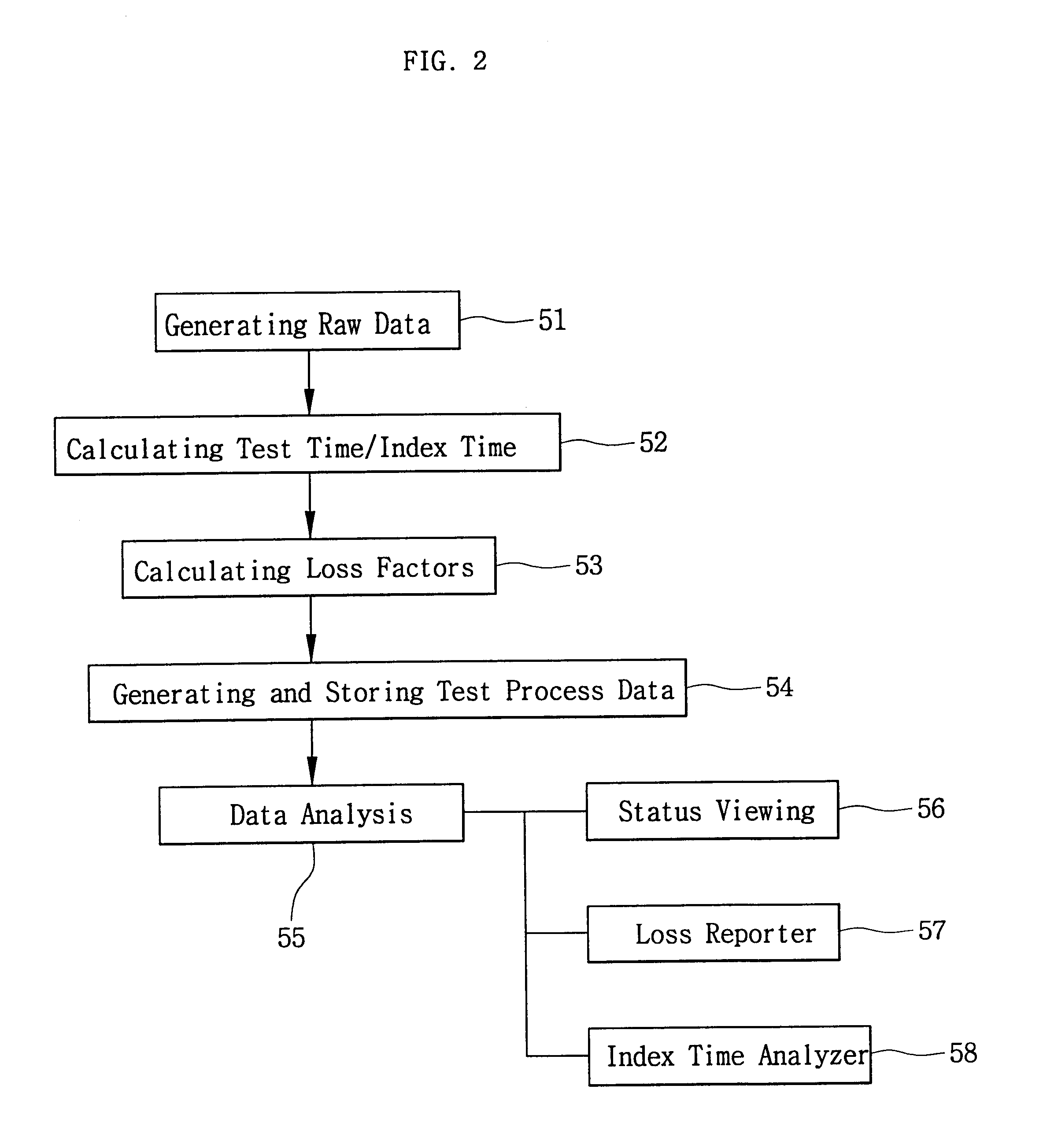
System and method for automatically analyzing and managing loss factors in test process of semiconductor integrated circuit devices
a technology of integrated circuit devices and loss factors, which is applied in the field of automatic analysis and management of loss factors in the test process, can solve the problems of increasing the cost and time of the test process, affecting the yield and productivity of ic devices, and being unreliable, so as to quickly deal with losses in the test process and improve the efficiency of the operation of the test system
- Summary
- Abstract
- Description
- Claims
- Application Information
AI Technical Summary
Benefits of technology
Problems solved by technology
Method used
Image

Examples
Embodiment Construction
devices.
[0024]FIG. 7 shows an exemplary user interface suitable for use in analyzing and managing loss factors in a test process of semiconductor integrated circuit devices.
[0025]FIG. 8 shows another exemplary user interface suitable for use in analyzing and managing loss factors in a test process of semiconductor integrated circuit devices.
[0026]FIG. 9 shows still another exemplary user interface suitable for use in analyzing and managing loss factors in a test process of semiconductor integrated circuit devices.
DETAILED DESCRIPTION OF PREFERRED EMBODIMENTS
[0027]Semiconductor IC devices are tested physically and / or electrically at numerous intervals during the overall fabrication process. However, the more critical tests of semiconductor devices are conducted during the latter portions of the fabrication and assembly processes. These test processes are commonly referred to as quality assurance (QA) tests and final testing of the devices. For ICs, these QA and final tests typically ...
PUM
 Abstract
Description
Claims
Application Information