Method for measuring semiconductor constituent element content and method for manufacturing a semiconductor device

a semiconductor and constituent element technology, applied in the direction of individual semiconductor device testing, semiconductor/solid-state device testing/measurement, instruments, etc., can solve the problems of inconvenient measurement at manufacturing sites, increased measurement error, and inability to meet the requirements of manufacturing, so as to achieve easy and accurate measurement of constituent element content and enhance manufacturing yields

Inactive Publication Date: 2005-02-22
PANASONIC CORP
View PDF3 Cites 13 Cited by
  • Summary
  • Abstract
  • Description
  • Claims
  • Application Information

AI Technical Summary

Benefits of technology

An object of the present invention is to provide a method for measuring the semiconductor constituent element content which will enable the easy and accurate measurement of the constituent element content of an SiGeC layer. Further, an object of the present invention is to provide a method for manufacturing a semiconductor device which can enhance manufacturing yields using the method.

Problems solved by technology

This is because measurement error tends to increase when measuring the constituent element content of an SiGeC layer, particularly.
However, large-scale devices, such as an X-ray diffraction device and a mass spectroscope, are required, making these methods inconvenient for measuring at manufacturing sites, and thus are not practical.

Method used


Image

  • Method for measuring semiconductor constituent element content and method for manufacturing a semiconductor device
  • Method for measuring semiconductor constituent element content and method for manufacturing a semiconductor device
  • Method for measuring semiconductor constituent element content and method for manufacturing a semiconductor device

Examples


Embodiment Construction

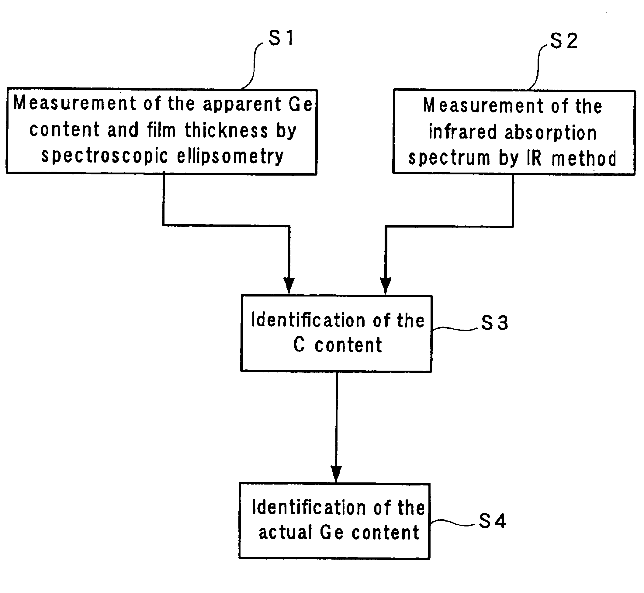
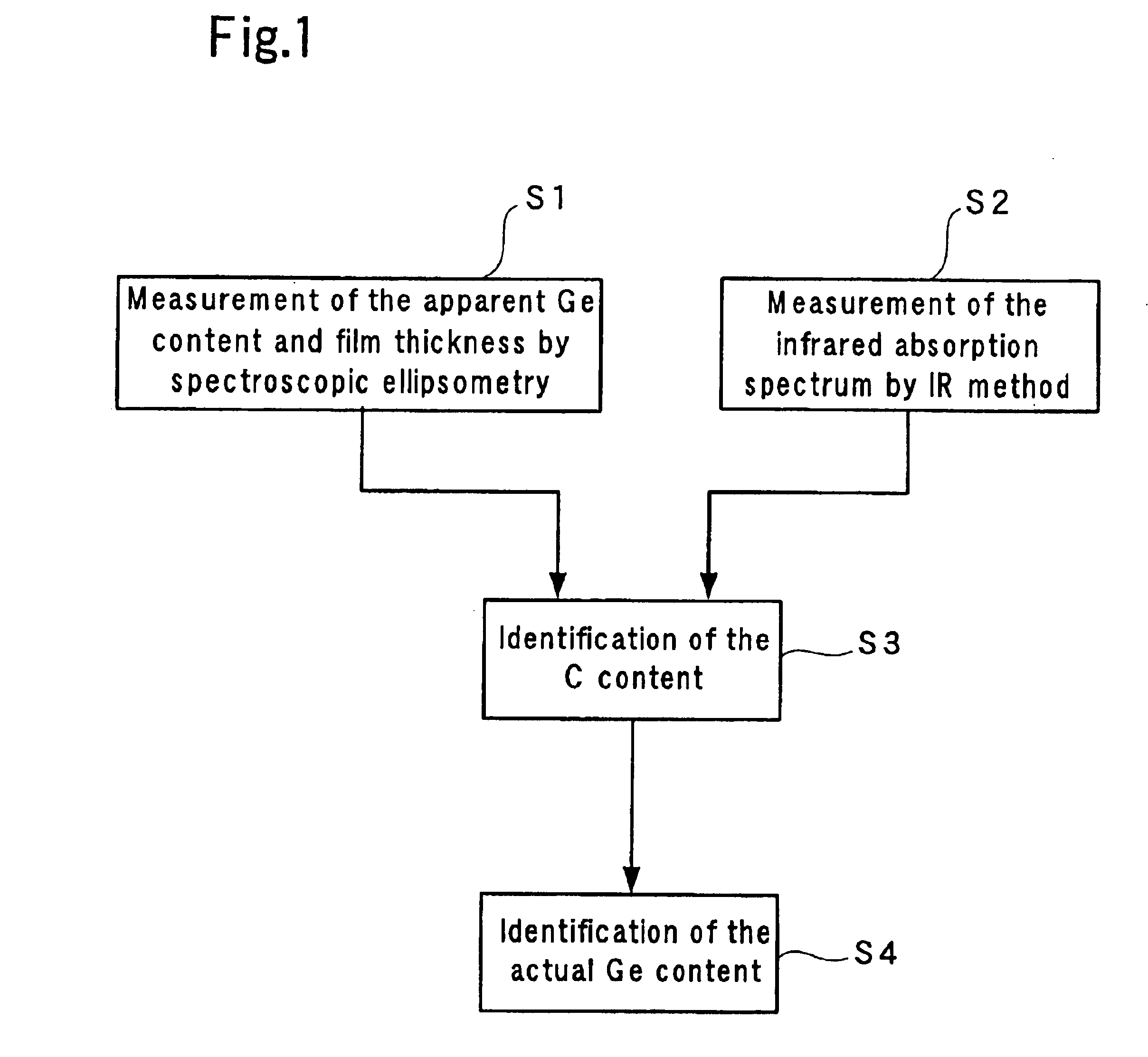
(Method for Measuring the Semiconductor Constituent Element Content)

Hereinafter, embodiments of the present invention will be described with reference to drawings. FIG. 1 is a flow chart illustrating a method for measuring semiconductor constituent element content according to one embodiment of the present invention. The present embodiment employs spectroscopic ellipsometry as the measurement method so as to calculate the apparent Ge content and film thickness of an SiGeC layer formed on a semiconductor substrate (Step 1).

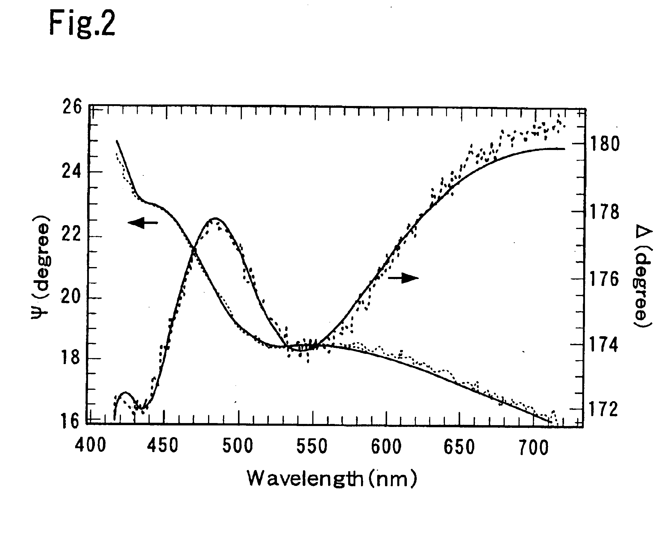
Spectroscopic ellipsometry is used to obtain information about a measurement sample by irradiating the sample with linearly polarized light, and measuring the change in the polarization states of the reflected light. The linearly polarized light has a P polarization component in which an electric-field vector is in parallel to the plane of incidence and an S polarization component in which an electric-field vector is perpendicular to the plane of incidence. When ea...


PUM

PropertyMeasurementUnit
incident angleaaaaaaaaaa
thickaaaaaaaaaa
sizeaaaaaaaaaa

Abstract

A method for measuring semiconductor constituent element content utilizes the steps of: obtaining a film thickness of an SiGeC layer formed on a semiconductor substrate by evaluation using spectroscopic ellipsometry; measuring infrared absorption spectrum of the SiGeC layer; and obtaining a C content of the SiGeC layer based on the film thickness and the infrared absorption spectrum of the SiGeC layer. The method: obtaining an apparent Ge content of the SiGeC layer by evaluation using spectroscopic ellipsometry; and obtaining an actual Ge content of the SiGeC layer based on the apparent Ge content and the C content. The constituent element content of the SiGeC layer can be easily and accurately measured according to the above-mentioned method.

Description

TECHNICAL FIELDThe present invention relates to a method for measuring semiconductor constituent element content, and a method for manufacturing a semiconductor device. More specifically, the present invention relates to a method for measuring the content of the elements that constitute an SiGeC layer and a method for manufacturing a semiconductor device having an SiGeC layer.BACKGROUND OF THE INVENTIONIn recent years, transistors having an SiGe layer or an SiGeC layer have received widespread attentions because such a transistor offers potential as an MIS transistor or a bipolar transistor which can operate at high speed. When manufacturing a semiconductor device having such a semiconductor layer, the film thickness and the constituent element content (for example, Ge content in the case of an SiGe layer, and Ge and C content in the case of an SiGeC layer) of the semiconductor layer must be controlled with high precision. Thus, these values must be calculated accurately during insp...

Claims


Application Information

Patent Timeline
Patent Type & Authority Patents(United States)
IPC IPC(8): G01N21/31G01N21/21G01N21/35
CPCG01N21/3563G01N21/211
Inventor KANZAWA, YOSHIHIKOSAITOH, TOHRUTAKAGI, TAKESHINOZAWA, KATSUYA
Owner PANASONIC CORP
Why Eureka
Try Eureka