

Low defect pre-emitter and pre-base oxide etch for bipolar transistors and related tooling
- Summary
- Abstract
- Description
- Claims
- Application Information
AI Technical Summary
Benefits of technology
Problems solved by technology
Method used
Image

Examples
Embodiment Construction
Vapor Phase Etching Process
(I) Process Sequence
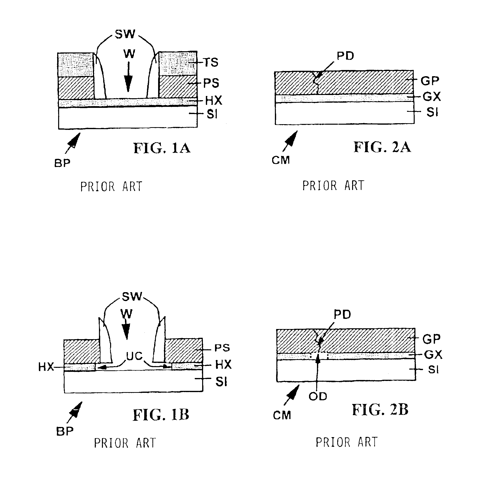
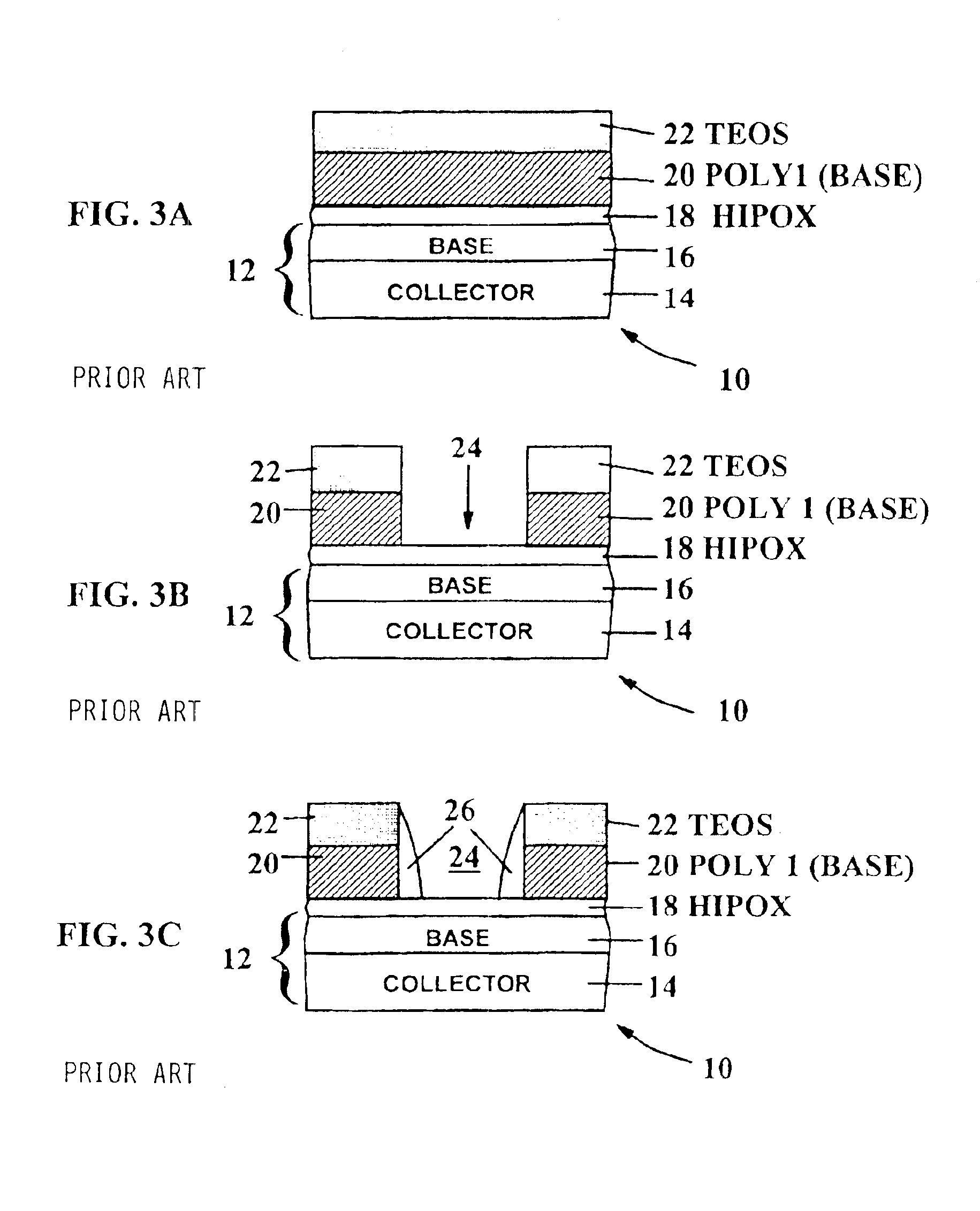
FIGS. 4A-4I illustrate a process of vapor phase etching (i.e. using a dry etching process) in accordance with an embodiment of this invention, when manufacturing the type of bipolar structure discussed above in connection with FIGS. 3A-3E. This process overcomes the problems of complete removal of the TEOS layer 22 and undercutting of the HIPOX layer 18.
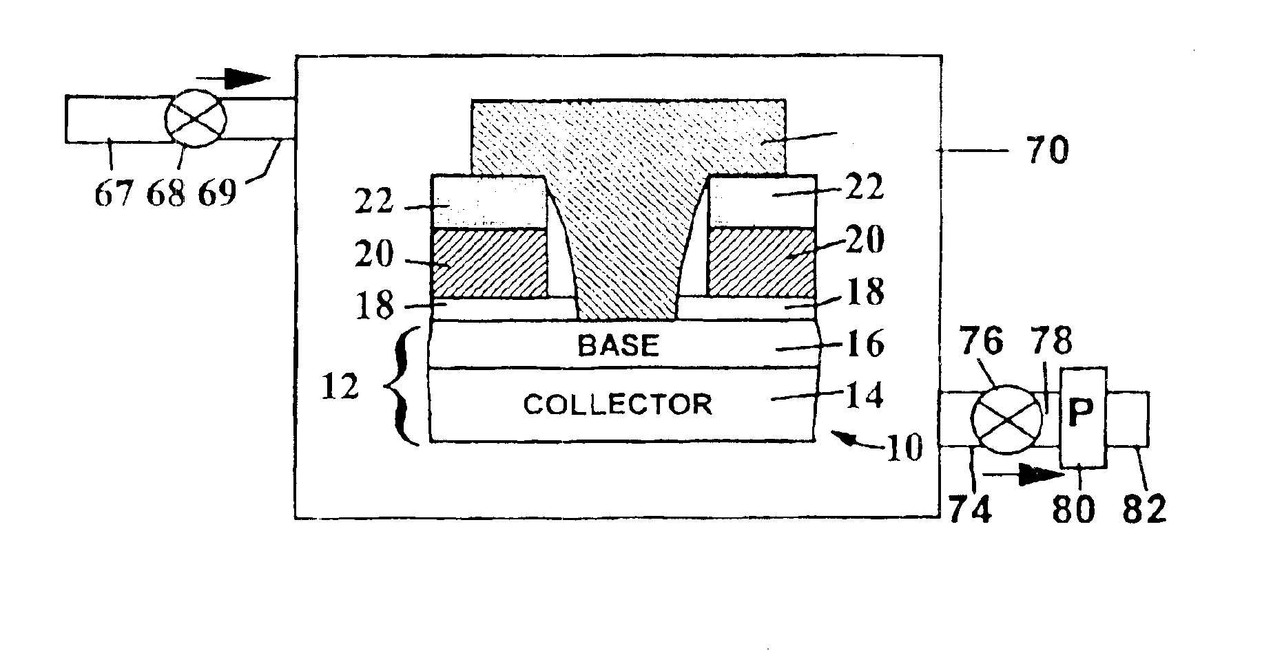
The structure formed in FIGS. 4A-4C is identical to FIGS. 3A-3C, with the same steps performed as described above, and with repeated reference numbers referring to identical elements.
FIG. 4D illustrates the result after commencing a step of precleaning of device 10 of FIG. 1A. The precleaning starts with introduction thereof into a sealed COR reaction chamber 44 in which a Chemical Oxide Removal (COR) process uses gas phase reactants to perform a self-limiting etch that is adjustable by controlling the parameters in the COR reaction chamber 44. The COR etching process employed in the pre...
PUM
 Abstract
Description
Claims
Application Information