

Image display apparatus and method of manufacturing the same
a technology of image display and assembly method, which is applied in the direction of identification means, tubes with screens, instruments, etc., can solve the problems of low vacuum attainable degree, low mass-productivity and properties reliability, and low exhaust speed, so as to achieve high air tight sealing structure and improve adhesion
- Summary
- Abstract
- Description
- Claims
- Application Information
AI Technical Summary
Benefits of technology
Problems solved by technology
Method used
Image

Examples
Embodiment Construction
An embodiment in which an image display apparatus according to this invention is applied to an FED will now be described in detail with reference to the drawings.
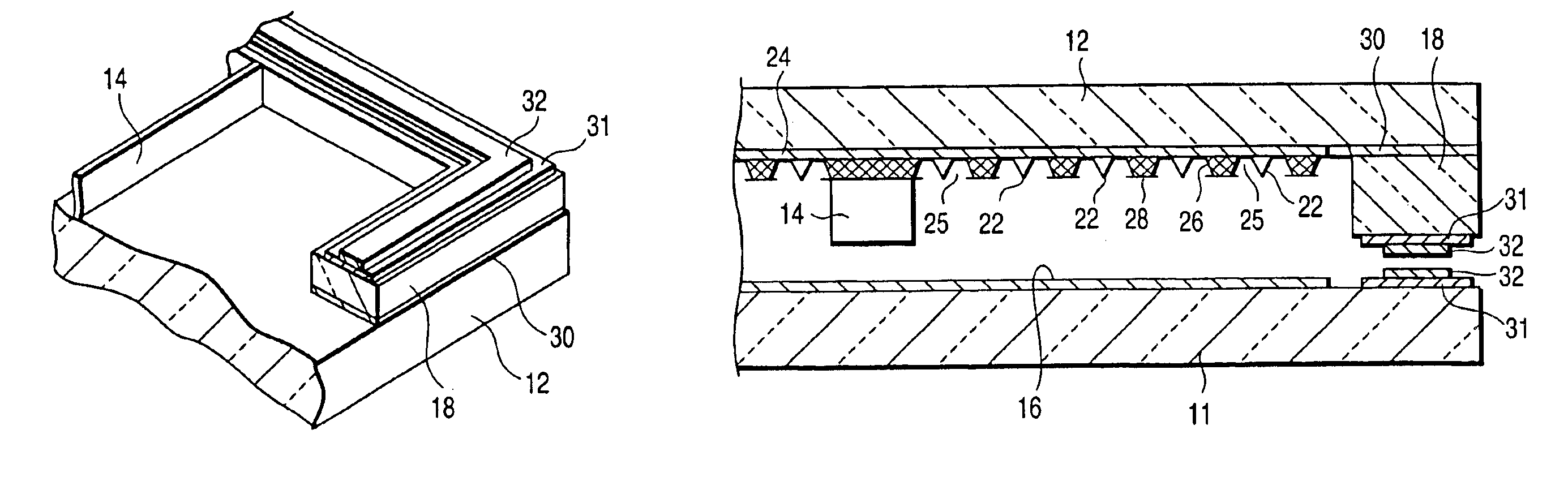
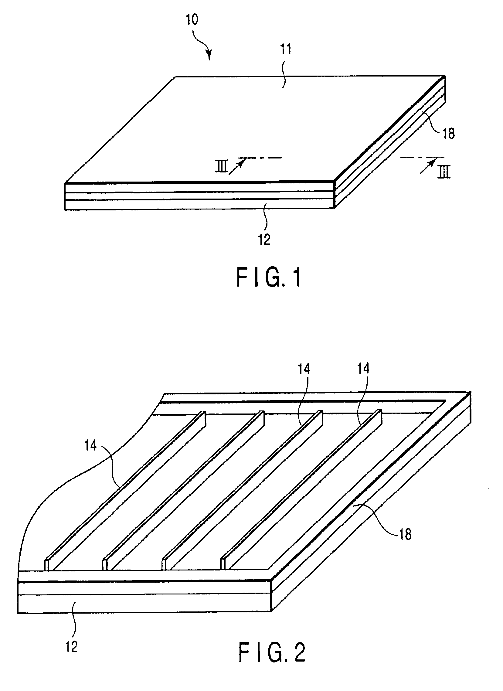
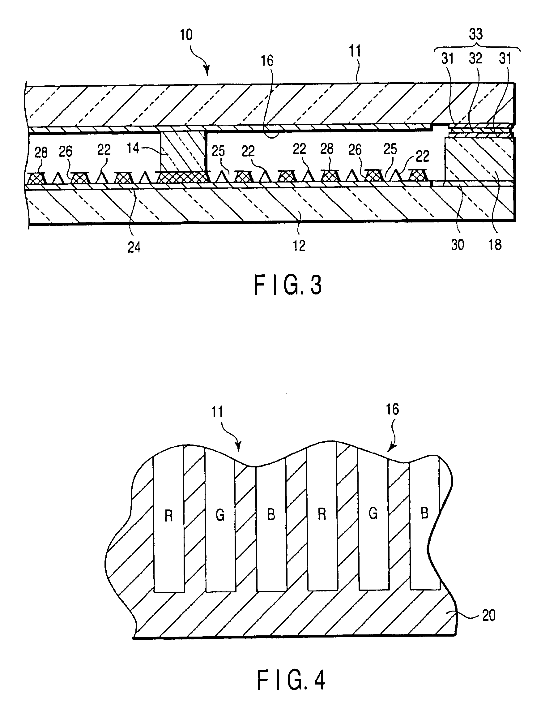
As shown in FIGS. 1 to 3, this FED comprises a front substrate 11 and a rear substrate 12 for use as insulating substrates, which are formed of rectangular glass plates, individually. These substrates 11 and 12 are opposed to each other with a gap of about 1.5 to 3.0 mm between them. The front substrate 11 and the rear substrate 12 have their respective peripheral edge portions joined together by means of a sidewall 18 in the form of a rectangular frame. They constitute a flat, rectangular vacuum envelope 10, the inside of which is kept at a vacuum.
The vacuum envelope 10 has therein a plurality of plate-shaped support members 14, which support an atmospheric load that acts on the rear substrate 12 and the front substrate 11. These support members 14 extend parallel to the short sides of the vacuum envelope 10 and are arrang...
PUM
 Abstract
Description
Claims
Application Information