Analog-digital conversion circuit

a conversion circuit and analog digital technology, applied in analogue/digital conversion, transmission systems, instruments, etc., can solve the problems of insufficient conversion accuracy and inability to achieve high area efficiency, and achieve the effect of reducing the load capacitance of the amplifier for each stage, high conversion operation, and improving the performance of the amplifier

Inactive Publication Date: 2005-02-22
SEMICON COMPONENTS IND LLC
View PDF6 Cites 19 Cited by
  • Summary
  • Abstract
  • Description
  • Claims
  • Application Information

AI Technical Summary

Benefits of technology

In this way, repeated uses of the first circuit allows a proceeding equivalent to a multi-stage pipeline structure to be formed. Consequently, the necessary area can be reduced.
In this case, the frequency dividing factor by the frequency divider in the phase locked loop is set by the frequency dividing factor setting device, so that the frequency of the first clock signal can readily be changed and the bit resolution can be changed as well.

Problems solved by technology

As the number of bits to convert has increased, however, sufficient conversion accuracy can no longer be obtained by the two-step flush method, and therefore an analog-digital conversion circuit having a multi-stage pipeline (step flush) structure has been developed.
However, in the analog-digital conversion circuit having the above described multi-stage pipeline structure, the area efficiency cannot be high.

Method used


Image

  • Analog-digital conversion circuit
  • Analog-digital conversion circuit
  • Analog-digital conversion circuit

Examples


Embodiment Construction

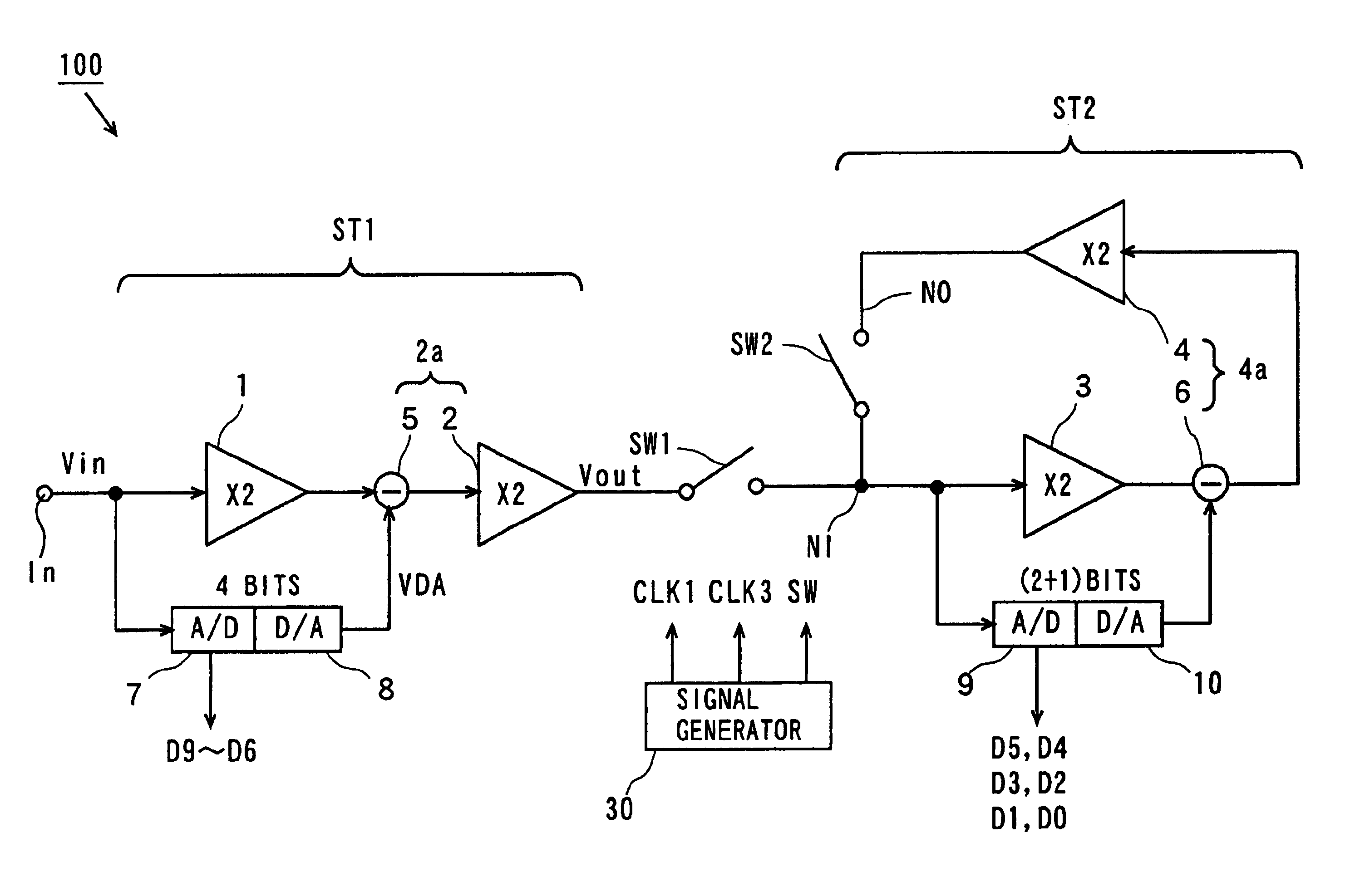
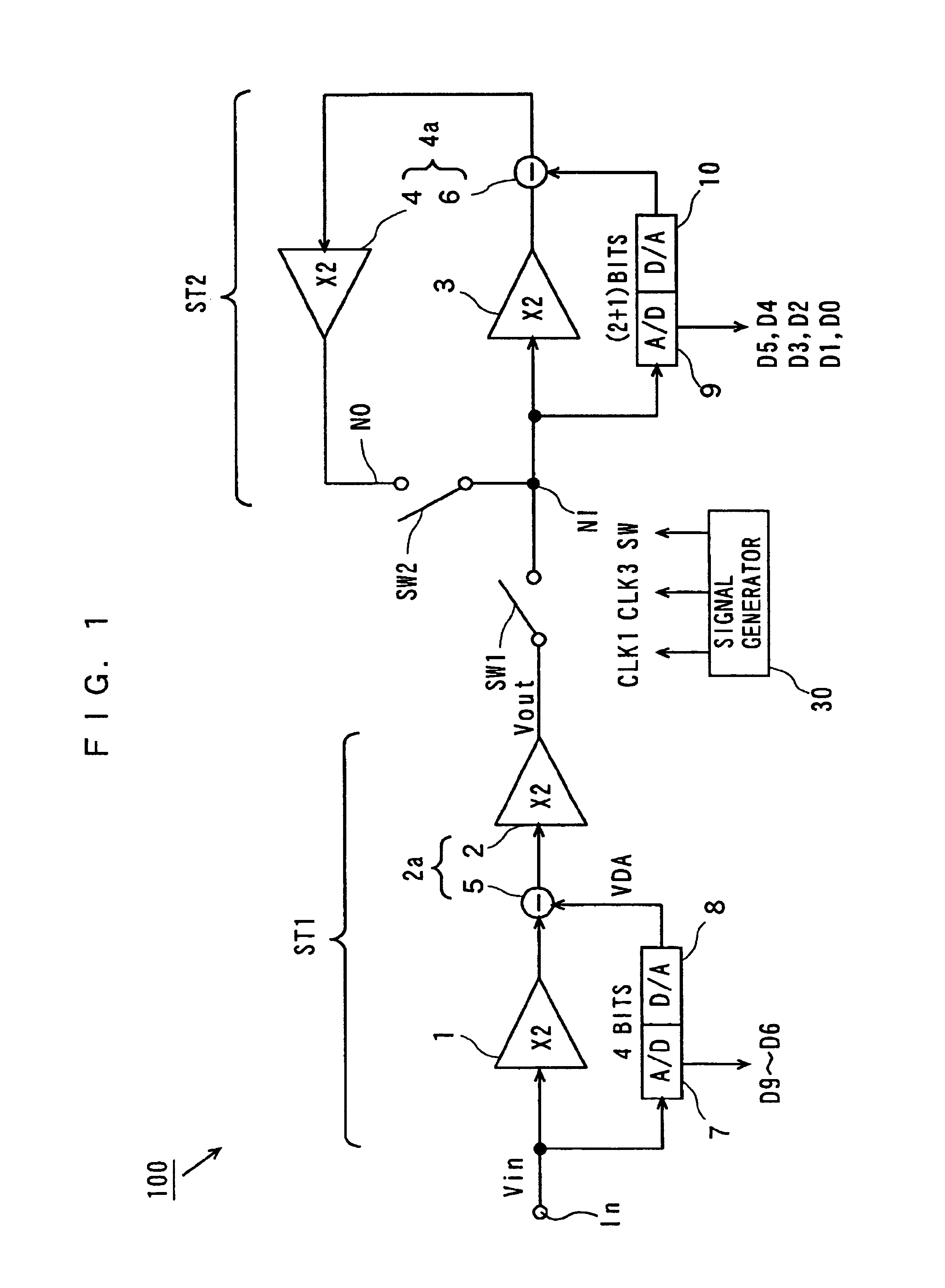
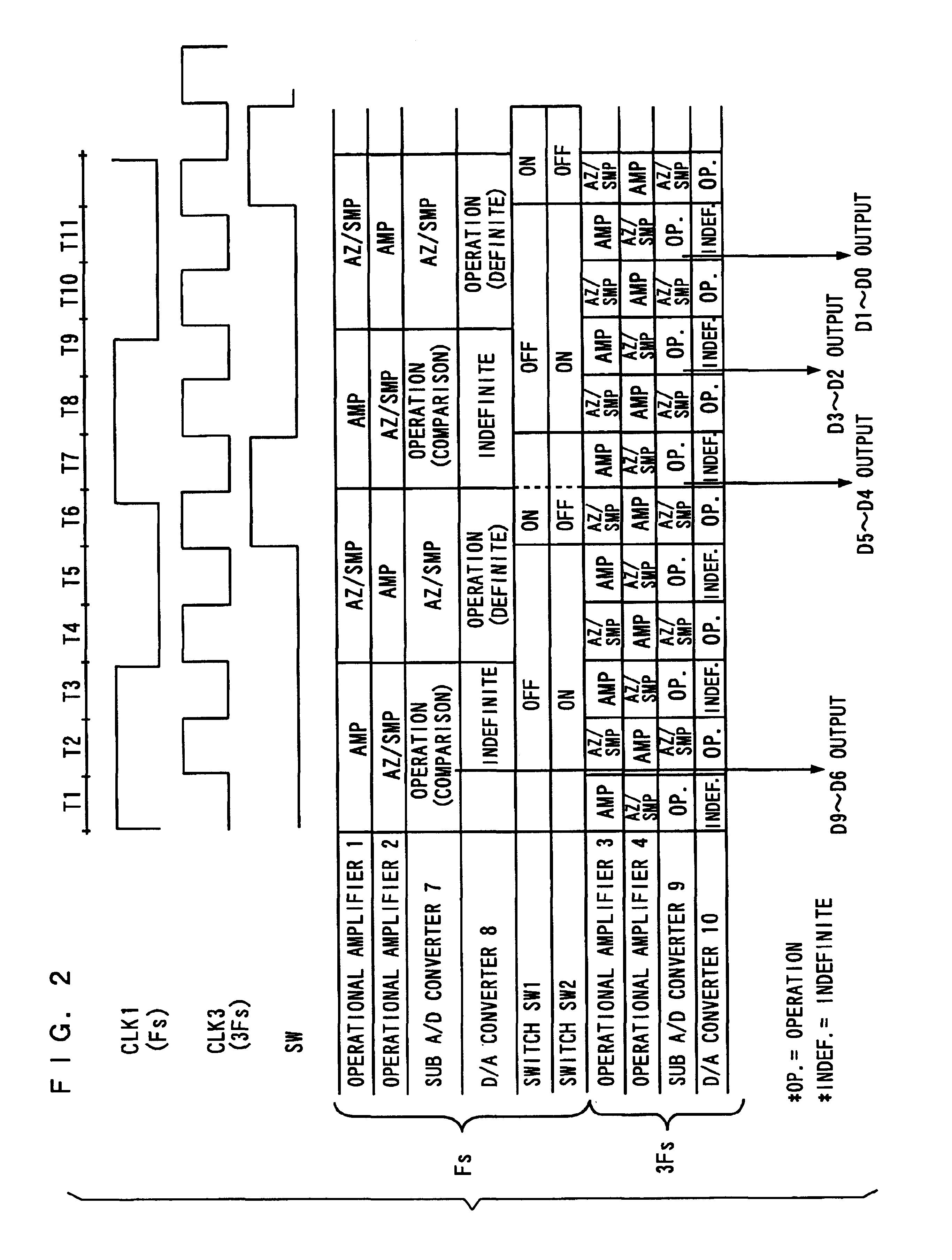
FIG. 1 is a block diagram of the configuration of an analog-digital conversion circuit according to one embodiment of the invention.

The analog-digital conversion circuit 100 in FIG. 1 includes a first stage circuit ST1, a second stage circuit ST2, switches SW1 and SW2, and a signal generator 30.

The first stage circuit ST1 includes an operational amplifier 1, a sub A / D converter 7, a D / A converter 8, a subtraction circuit 5, and an operational amplifier 2. The subtraction circuit 5 and the operational amplifier 2 form a differential amplifier 2a. The second stage circuit ST2 includes an operational amplifier 3, a sub A / D converter 9, a D / A converter 10, a subtraction circuit 6, and an operational amplifier 4. The subtraction circuit 6 and the operational amplifier 4 form a differential amplifier 4a.

The operational amplifiers 1 and 2 in the first stage circuit ST1 and the operational amplifiers 3 and 4 in the second stage circuit ST2 each have a gain of 2. The operational amplifier 1...


PUM


Abstract

An operational amplifier, a sub A / D converter, a D / A converter, and an operation amplifier in a first stage circuit operate in response to a clock signal. An operation amplifier, a sub A / D converter, a D / A converter, and an operation amplifier in a second stage circuit operate in response to a clock signal having a frequency three times as high as that of the first clock signal. An analog signal output from the operational amplifier in the first stage is applied to an input node in the second stage circuit through a switch. An analog signal output from an operational amplifier in the second stage circuit is applied to an input node in the second stage circuit through a switch.

Description

BACKGROUND OF THE INVENTION1. Field of the InventionThe present invention relates to an analog-digital conversion circuit having a multi-stage pipeline (step flush) structure.2. Description of the Background ArtIn recent years, with the advent of advanced digital processing technology for video signals, there has been a growing demand for digital-analog conversion circuits (A / D converters) for processing video signals. Since the analog-digital conversion circuit for processing video signals must operate at high speed, a two-step flush (a two-step parallel) method has been widely employed for conventional analog-digital conversion circuits.As the number of bits to convert has increased, however, sufficient conversion accuracy can no longer be obtained by the two-step flush method, and therefore an analog-digital conversion circuit having a multi-stage pipeline (step flush) structure has been developed. (See, for example, Japanese Patent Laid-Open No. 11-88172).FIG. 12 is a block diag...

Claims


Application Information

Patent Timeline
Patent Type & Authority Patents(United States)
IPC IPC(8): H03M1/14H03M1/16H03M1/44
CPCH03M1/167H03M1/162
Inventor WADA, ATSUSHITANI, KUNIYUKI
Owner SEMICON COMPONENTS IND LLC
Why Eureka
Try Eureka