Surface-emitting semiconductor laser and method of manufacturing the same

a semiconductor laser and surface-emitting technology, applied in the direction of lasers, semiconductor lasers, optical resonator shape and construction, etc., can solve the problems of interfering with the achievement of rapid drive or compact devices, and achieve the effect of excellent light emission efficiency, rapid drive and compact devices

Inactive Publication Date: 2005-02-22
SEIKO EPSON CORP
View PDF7 Cites 5 Cited by
  • Summary
  • Abstract
  • Description
  • Claims
  • Application Information

AI Technical Summary

Benefits of technology

The object of the present invention is the provision of a surface-emitting semiconductor laser and method of manufacture thereof of excellent efficiency of light emission, and allowing rapid drive and a compact device to be achieved.
According to the surface emission laser of the present invention, by forming the contact region in the non-light-emitting region, the influence of light absorption and dispersion occurring in the contact region on the efficiency of light emission of the resonator can be reduced, and therefore laser light can be emitted without lowering the efficiency of light emission. Furthermore, mounting using the wire bonding that is in general use is not required, and since it is possible to form a pair of electrodes in a single plane of the semiconductor substrate, rapid drive and a compact device can be achieved.
Furthermore, the contact region may have a higher carrier density than the layer including the first mirror. According to this configuration, excellent ohmic contact can be obtained, and an element having excellent efficiency of light emission can be implemented.
Moreover, the first and second electrodes may be formed in substantially the same plane. According to this configuration, rapid drive is possible, and excellent electrodes of low breakage and low parasitic capacitance can be formed. For example, bumps or the like can easily be formed on the first electrode and the second electrode.
(3) The carrier density in the contact region may be at least 5×1018 cm−3. According to this configuration, excellent ohmic contact can be obtained.
According to the method of manufacturing a surface-emitting semiconductor laser of the present invention, a surface-emitting semiconductor laser of excellent efficiency of light emission, and allowing rapid drive and a compact device to be achieved can be obtained by a convenient method.

Problems solved by technology

However, mounting using this manner of wire bonding may interfere with the achievement of rapid drive or a compact device.

Method used


Image

  • Surface-emitting semiconductor laser and method of manufacturing the same
  • Surface-emitting semiconductor laser and method of manufacturing the same
  • Surface-emitting semiconductor laser and method of manufacturing the same

Examples


first embodiment

(Device Configuration)

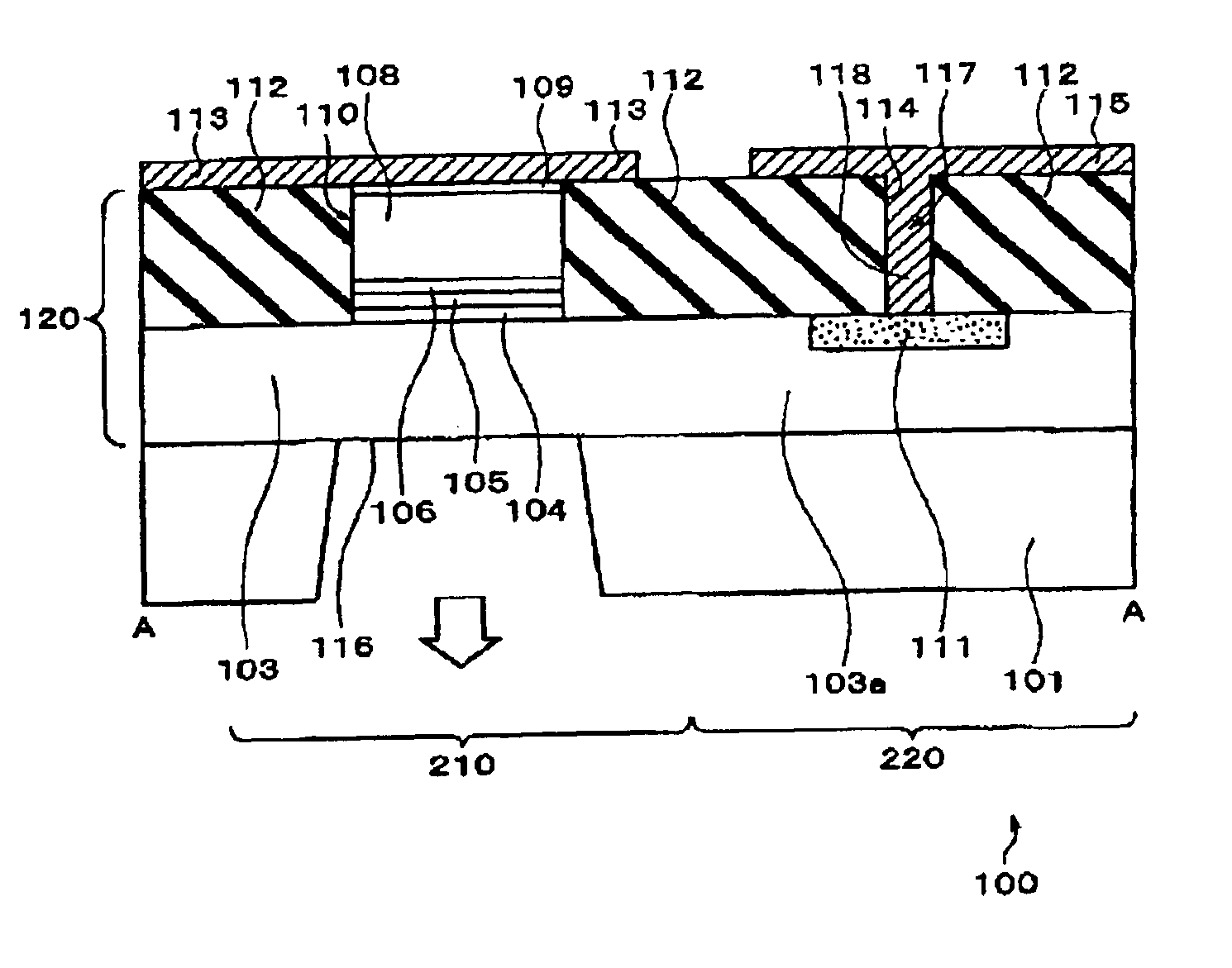
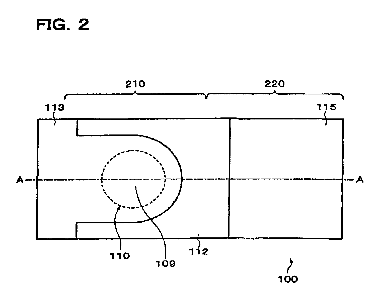
First, the configuration of the first embodiment of the surface-emitting semiconductor laser 100 (hereinafter referred to as “surface emission laser”) of the present invention is described using FIGS. 1 and 2. FIG. 1 illustrates schematically a section of the first embodiment of the surface emission laser 100 of the present invention, and is a section taken along the line A—A in FIG. 2. FIG. 2 is a plan view schematically showing the surface emission laser 100 shown in FIG. 1.

The surface emission laser 100 is constituted by a light-emitting region 210 and a non-light-emitting region 220. In the light-emitting region 210, a resonator 120 is formed. The resonator 120 is formed on a semiconductor substrate 101, being for example a GaAs substrate. In this embodiment, the case is shown in which in the light-emitting region 210, in at least a part of the resonator 120 a pillar portion 110 is formed. The resonator 120 is formed by lamination in sequence of a buffer la...

first modification

(First Modification)

FIG. 8 is a sectional view of a first modification of this embodiment of the surface emission laser.

In the surface emission laser 100 shown in FIG. 1, the case has been described that the contact region 111 and second electrode 115 are contacted with the contact portion 117 interposed, but as in the surface emission laser 200 shown in FIG. 8, the contact region 111 and a second electrode 215 can be directly contacted without a contact portion interposed. Except for the fact that no contact portion is provided, and the portion of the insulating layer 212 formed on the first mirror 103 and the layer 103a linking to the first mirror 103 which is positioned over the portion forming the contact region 111 is removed, after which the second electrode 215 is directly formed on this portion, the surface emission laser 200 shown in FIG. 8 is obtained by a substantially similar process as the surface emission laser 100 shown in FIG. 1, and substantially the same effect and...

second embodiment

(Device Configuration)

Next, the configuration of a second embodiment of a surface emission laser 300 of the present invention is described with reference to FIG. 9. FIG. 9 shows schematically a section through the second embodiment of the surface emission laser 300 of the present invention.

The surface emission laser 300 shown in FIG. 9 differs in configuration from the first embodiment of the surface emission laser 100 in that an insulating layer 312 is formed to extend along the side surface of the pillar portion 110 and the top surface of the resonator 120. On the other hand, the surface emission laser 300 shown in FIG. 9 has, like the surface emission laser 100 shown in FIG. 1, the contact region 111 and a second electrode 315 electrically connected with a contact portion 317 interposed. Since other portions of the configuration are substantially the same as those of the first embodiment of the surface emission laser 100, for those portions of the surface emission laser 300 of th...


PUM


Abstract

A surface-emitting semiconductor laser having a light-emitting region and a non-light-emitting region, the light-emitting region emitting light in a direction perpendicular to a semiconductor substrate. The light-emitting region includes a resonator formed on the semiconductor substrate. The non-light-emitting region includes a contact region electrically connected to the resonator. The contact region is formed in a layer which is part of a layer including at least part of the resonator but is apart from the part of the resonator, and the contact region has a higher carrier density than the layer in which the contact region is formed.

Description

Japanese Patent Application No. 2001-208192, filed on Jul. 9, 2001, is hereby incorporated by reference in its entirety.BACKGROUND OF THE INVENTIONThe present invention relates to a surface-emitting semiconductor laser of excellent efficiency of light emission, and capable of achieving a rapid drive and compact device, and a method of manufacturing the same.A surface-emitting semiconductor laser is a light-emitting element capable of integration in two dimensions, and is anticipated as the next generation high-speed and large capacity light source, for application to optical parallel communications and optical parallel computation, laser beam printers, and the like.Such a surface-emitting semiconductor laser generally has a resonator formed on a semiconductor substrate, and this resonator is driven by passing a current in the direction perpendicular to the semiconductor substrate. Since this surface-emitting semiconductor laser has a current flowing in the direction perpendicular to...

Claims


Application Information

Patent Timeline
Patent Type & Authority Patents(United States)
IPC IPC(8): H01S5/00H01S5/183H01L27/15H01S5/042
CPCB82Y20/00H01S5/18305H01L27/15H01S5/0207H01S2301/176H01S5/18341H01S5/3432H01S5/0422
Inventor KANEKO, TSUYOSHI
Owner SEIKO EPSON CORP
Why Eureka
Try Eureka