Apparatus and methods for determining and localization of failures in test structures using voltage contrast

a technology of voltage contrast and test structure, applied in the direction of basic electric elements, semiconductor/solid-state device testing/measurement, instruments, etc., can solve the problems of large number of fabrication steps, time-consuming and expensive, and large number of processing steps before yield loss determination

Inactive Publication Date: 2005-03-01
KLA TENCOR TECH CORP
View PDF36 Cites 105 Cited by
  • Summary
  • Abstract
  • Description
  • Claims
  • Application Information

AI Technical Summary

Problems solved by technology

Unfortunately, the fabrication of the SRAM cell requires a large number of processing steps.
Such extensive number of fabrication steps before yield loss may be determined is very time consuming.
An additional problem with the SRAM test structure is that even though the electrical defect is localized to a certain cell, it does not localize the failing layer.
Failure analysis of the defective cell requires layer by layer deprocessing, which is also time consuming and expensive.

Method used


Image

  • Apparatus and methods for determining and localization of failures in test structures using voltage contrast
  • Apparatus and methods for determining and localization of failures in test structures using voltage contrast
  • Apparatus and methods for determining and localization of failures in test structures using voltage contrast

Examples


Embodiment Construction

Reference will now be made in detail to a specific embodiment of the invention. An example of this embodiment is illustrated in the accompanying drawings. While the invention will be described in conjunction with this specific embodiment, it will be understood that it is not intended to limit the invention to one embodiment. On the contrary, it is intended to cover alternatives, modifications, and equivalents as may be included within the spirit and scope of the invention as defined by the appended claims. In the following description, numerous specific details are set forth in order to provide a thorough understanding of the present invention. The present invention may be practiced without some or all of these specific details. In other instances, well known process operations have not been described in detail in order not to unnecessarily obscure the present invention.

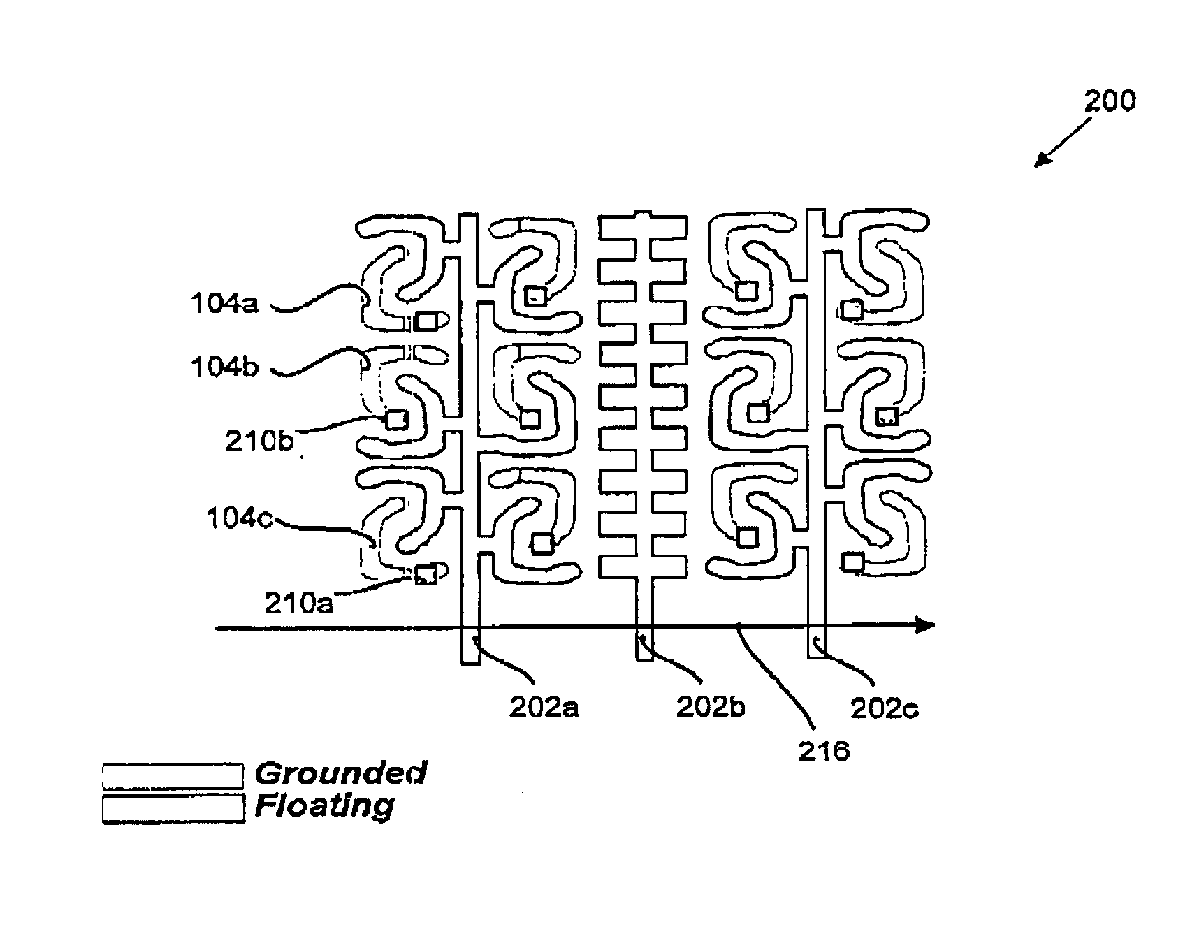
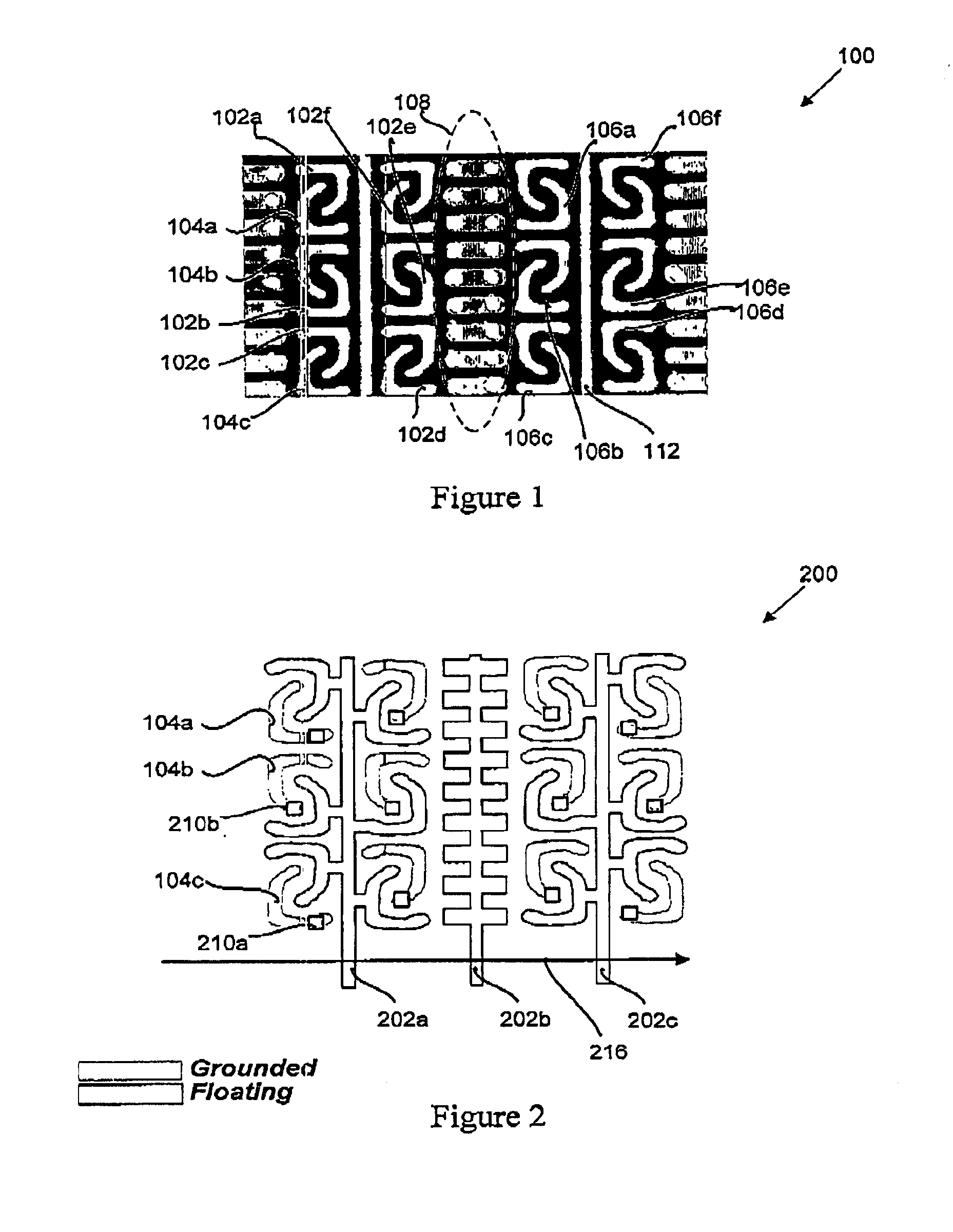
The SRAM test vehicle we describe here overcomes the limitations described above. Although the present invention i...


PUM


Abstract

Disclosed is test structure that can be fabricated with minimal photolithography masking steps and in which defects may be localized to specific layers. Mechanisms for fabricating such test structures are also provided. In one embodiment, a semiconductor test structure suitable for a voltage contrast inspection is provided. The test structure includes one or more test layers corresponding to one or more product layers selected from a plurality of product layers of an integrated circuit (IC) product structure. The number of the selected one or more test layers is less than a total number of the plurality of product layers of the product structure, and the test layers include at least a first portion that is designed to have a first potential during the voltage contrast inspection and a second portion that is designed to have a second potential during the voltage contrast inspection. The first potential differs from the second potential. The selected one or more test layers which correspond to product layers are selected from the plurality of product layers such that defects found in the test layers of the test structure during the voltage contrast inspection represent a prediction of defects in the corresponding product structure.

Description

BACKGROUND OF THE INVENTIONAn SRAM cell array is a common test structure used in yield ramp. This is due to its ability to localize defects to within a given cell.Unfortunately, the fabrication of the SRAM cell requires a large number of processing steps. For example, an isolation layer is formed, gates are patterned, junctions are patterned and formed, etc. Although most of the yield loss occurs as a result of the backend steps, the front-end steps must also be completed to make functioning SRAM blocks. Thus, all the backend processing, typically including three layers of metal and the passivation layer for the pads, must also be done before the devices can be tested electrically. Such extensive number of fabrication steps before yield loss may be determined is very time consuming.An additional problem with the SRAM test structure is that even though the electrical defect is localized to a certain cell, it does not localize the failing layer. Failure analysis of the defective cell ...

Claims


Application Information

Patent Timeline
Patent Type & Authority Patents(United States)
IPC IPC(8): H01L23/58G01R31/28G01R31/307H01L23/544
CPCH01L22/34G01R31/2884G01R31/307
Inventor WEINER, KURT H.VERMA, GAURAVNUNAN, PETER D.DE, INDRANIL
Owner KLA TENCOR TECH CORP
Why Eureka
Try Eureka