SRAM control circuit with a power saving function

a control circuit and function technology, applied in the direction of digital storage, instruments, computing, etc., can solve the problems of requiring not only the operating speed but also the low power consumption, and the cost of sram is much higher than dram, so as to reduce the power consumption of sram read operation.

Inactive Publication Date: 2005-03-01
SUNPLUS TECH CO LTD
View PDF1 Cites 11 Cited by
  • Summary
  • Abstract
  • Description
  • Claims
  • Application Information

AI Technical Summary

Benefits of technology

An object of the present invention is to provide an SRAM control circuit with a power saving function, which can reduce power consumption on SRAM read operation.

Problems solved by technology

In addition, SRAM costs much higher and consumes more power than DRAM.
However, in recent years, portable devices are in wide spread use, which require not only the operating speed but also low power consumption.

Method used


Image

  • SRAM control circuit with a power saving function
  • SRAM control circuit with a power saving function
  • SRAM control circuit with a power saving function

Examples


Embodiment Construction

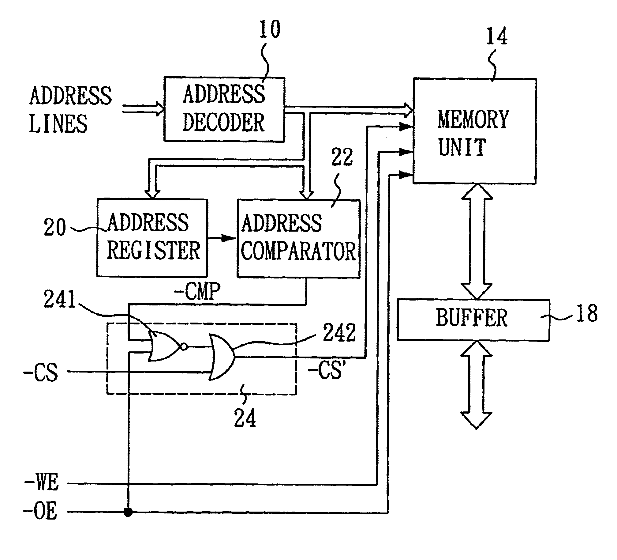
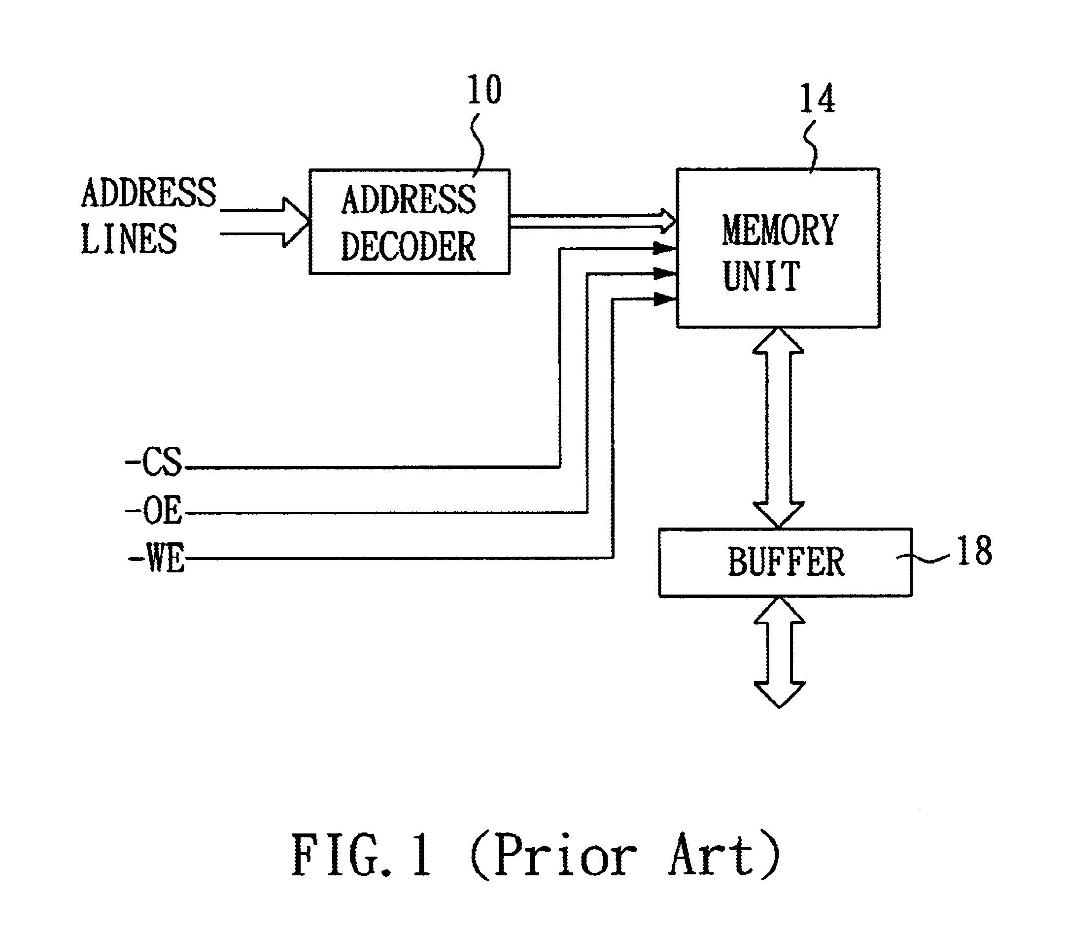
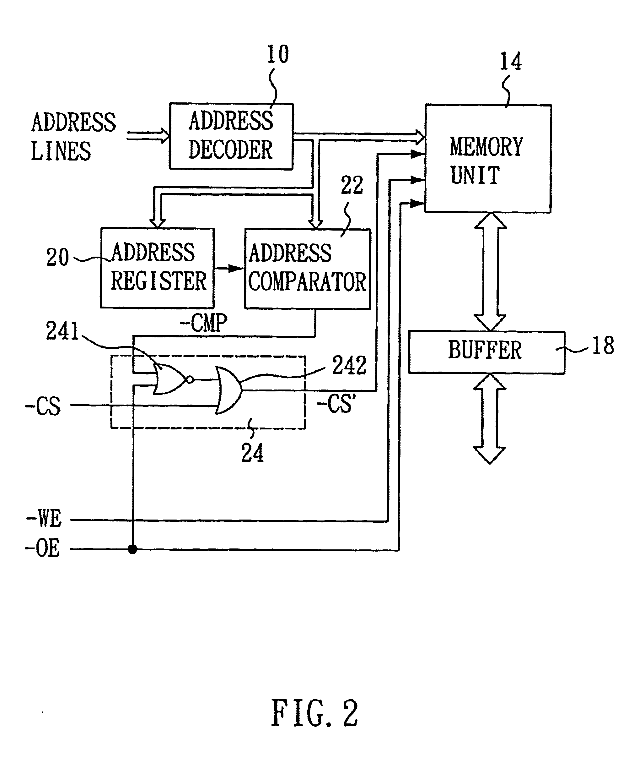
With reference to FIG. 2, a preferred embodiment of SRAM control circuit with a power saving function in accordance with the present invention is shown, wherein, same as in the prior art, all control signals are active low, i.e., enabled at low level and disabled at high level. As shown in FIG. 2, a read operation is performed when the chip select signal ˜CS and the output enable signal ˜OE are active (logic 0), and a write operation is performed when the chip select signal ˜CS and the write enable signal ˜WE are active (logic 0).

As shown in FIG. 2, the inventive SRAM control circuit with a power saving function includes an address decoder 10, an address register 20, an address comparator 22, a memory unit 14, a buffer 18 and a mask logic 24. The address decoder 10 reads the address on address lines and decodes the address to output an address signal to select a specific memory area in the memory unit 14.

The address register 20 stores the current address and outputs a previous addre...


PUM


Abstract

An SRAM control circuit with a power saving function is disclosed, which uses an address comparator to compare a current address and a previous address in an SRAM read operation. When the two addresses are the same, data is outputted directly from a buffer without enabling a memory unit, thereby saving power.

Description

BACKGROUND OF THE INVENTION1. Field of the InventionThe present invention relates to a static random access memory (SRAM) control circuit and, more particularly, to an SRAM control circuit with a power saving function.2. Description of Related ArtIn general, memory can be divided into two types, SRAM and DRAM (dynamic access memory). Upon the same chip area, DRAM normally is more than four times the capability of SRAM but SRAM is more than four times the speed of DRAM. In addition, SRAM costs much higher and consumes more power than DRAM. Therefore, for the balance between memory price and performance in computer design, SRAM for use as a cache memory is generally provided between the central processing unit (CPU) and DRAM, thereby providing a cache function.FIG. 1 is a schematic diagram of a typical SRAM structure. As shown in FIG. 1, an address decoder 10 reads and decodes data on address lines in order to output an address signal to select a specific memory area in a memory unit ...

Claims


Application Information

Patent Timeline
Patent Type & Authority Patents(United States)
IPC IPC(8): G06F12/00G11C7/00G11C5/00G11C11/413
CPCG11C11/413
Inventor CHEN, GENG-LIN
Owner SUNPLUS TECH CO LTD
Why Eureka
Try Eureka