Manufacturing method of semiconductor device
a manufacturing method and semiconductor technology, applied in semiconductor devices, semiconductor/solid-state device details, electrical devices, etc., can solve the problem of unavoidable cost increas
- Summary
- Abstract
- Description
- Claims
- Application Information
AI Technical Summary
Problems solved by technology
Method used
Image


Examples
first embodiment
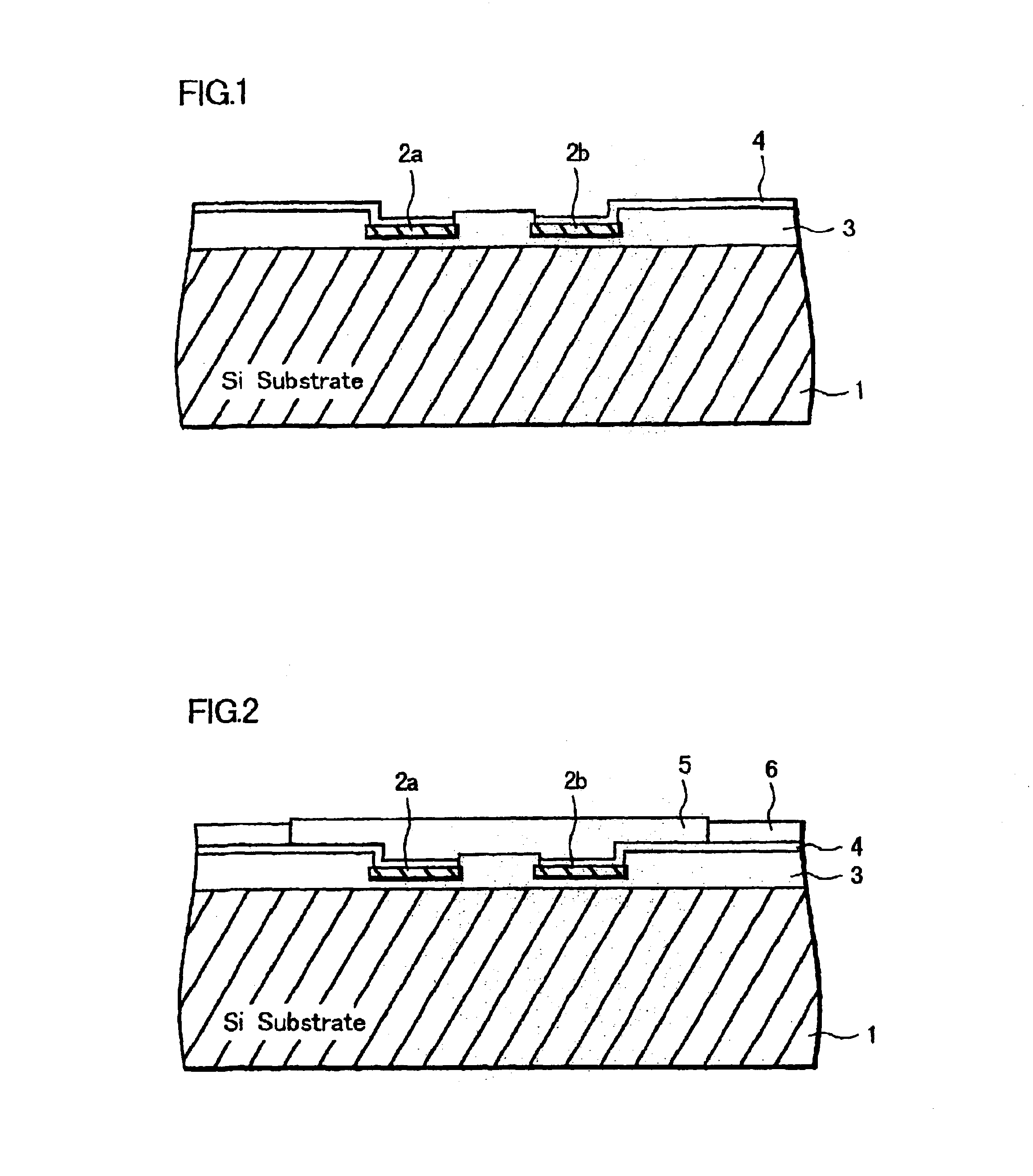
The first embodiment according to the manufacturing method of the semiconductor device of this invention will be explained referring to the figures hereinafter.
First, an oxide film is formed on a silicon wafer (hereafter referred to as Si substrate) having a thickness of 1 to 600 μm, a plurality of metal (aluminum, aluminum alloy or copper, for example) pads 2a and 2b are formed on the oxide film, and an SiO2 film or a PSG (phosphosilicate glass) film is formed by plasma CVD to cover the pads 2a and 2b, forming a first oxide film 3 of a predetermined thickness together with the oxide film, as shown in FIG. 1. The pads 2a and 2b are connected with corresponding semiconductor elements formed in the Si substrate 1. The first oxide film 3 may be ground physically or etched chemically, for example, when extra flatness is required. Then portions (surface portions) of the pads 2a and 2b are exposed by etching the first oxide film 3 on the pads 2a and 2b using a photoresist film (not shown)...
third embodiment
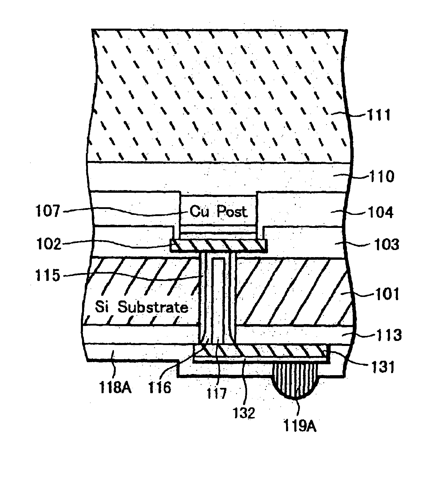
The third embodiment according to the manufacturing method of the semiconductor device of this invention will be explained referring to figures hereinafter.
First, an oxide film is formed on a silicon wafer (hereafter referred to as Si substrate) 101 of 600 μm in thickness, a metal (Al, Al alloy or copper, for example) pad 102 is formed on the oxide film, and an SiO2 film or a PSG film is formed by plasma CVD to cover the pad 102, forming a first oxide film 103 of a predetermined thickness together with the oxide film, as shown in FIG. 10A. The pad 102 is connected with a semiconductor element formed in the Si substrate 101. The first oxide film 103 may be ground physically or etched chemically, for example, when extra flatness is required. Then a portion (surface portion) of the pad 102 is exposed by etching the first oxide film 103 on the pad 102 using a photoresist film (not shown) as a mask. Total thickness of the first oxide film 103 is about 5 μm in this embodiment.
Next, a poly...
PUM
 Abstract
Description
Claims
Application Information
 - Generate Ideas
- Intellectual Property
- Life Sciences
- Materials
- Tech Scout
- Unparalleled Data Quality
- Higher Quality Content
- 60% Fewer Hallucinations
Browse by: Latest US Patents, China's latest patents, Technical Efficacy Thesaurus, Application Domain, Technology Topic, Popular Technical Reports.
© 2025 PatSnap. All rights reserved.Legal|Privacy policy|Modern Slavery Act Transparency Statement|Sitemap|About US| Contact US: help@patsnap.com