Post-passivation thick metal pre-routing for flip chip packaging

a technology of flip chip and prerouting layer, which is applied in the direction of electrical equipment, semiconductor devices, semiconductor/solid-state device details, etc., can solve the problems of increasing the ic pin count and the substrate unit cost, and achieve the effect of reducing the number of routing layers on the substrate and not affecting the performance of the ic chip

Inactive Publication Date: 2005-03-08
ALTERA CORP
View PDF2 Cites 66 Cited by
  • Summary
  • Abstract
  • Description
  • Claims
  • Application Information

AI Technical Summary

Benefits of technology

In summary, the present invention is a semiconductor package comprising an IC chip and a substrate, wherein part of the substrate routing such as substrate level trace routing is placed on the IC chip using post-passivation thick metal process at wafer level. Therefore, the I / O pads on the IC chip are not only redistributed but are also pre-routed using conductive pre-routing lines on the chip for the purpose of reducing the number of routing layers on the substrate. The pre-routing lines are made of post-passivation metal that is sufficiently thick so that the resistence and inductance associated with the pre-routing lines are sufficiently small and the performance of the IC chip is not affected. Depending on the density of the pads on the IC chip, multiple layers of pre-routing lines may be required.

Problems solved by technology

However, with increasing IC complexity, the IC pin count has also increased drastically, so that if only peripheral pads were used, pitches that are less than 60 micron would be necessary.
The substrate unit cost increases drastically due to the additional layer count and advanced design rules to lay out the substrate routing lines.

Method used


Image

  • Post-passivation thick metal pre-routing for flip chip packaging
  • Post-passivation thick metal pre-routing for flip chip packaging
  • Post-passivation thick metal pre-routing for flip chip packaging

Examples


Embodiment Construction

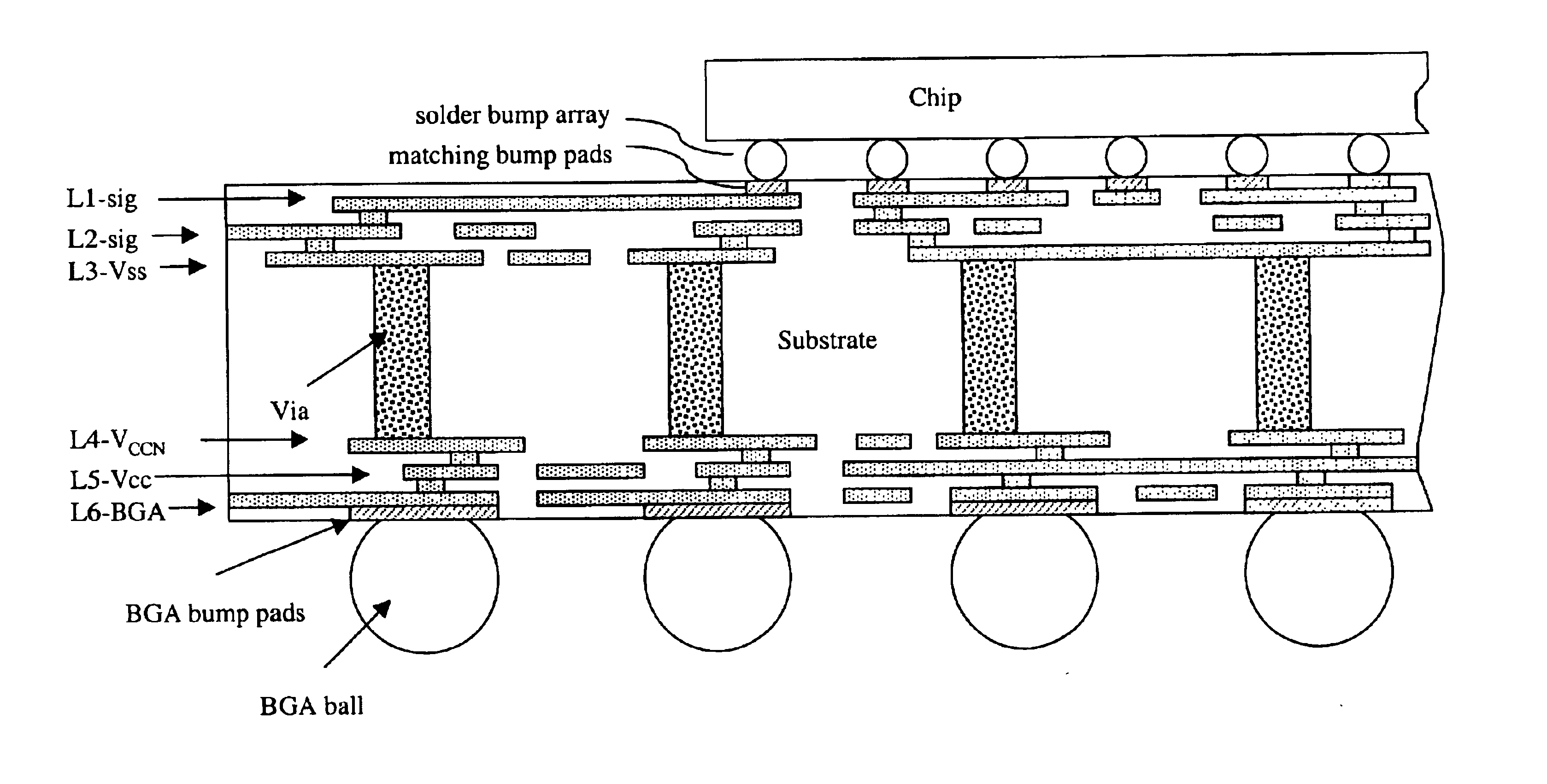
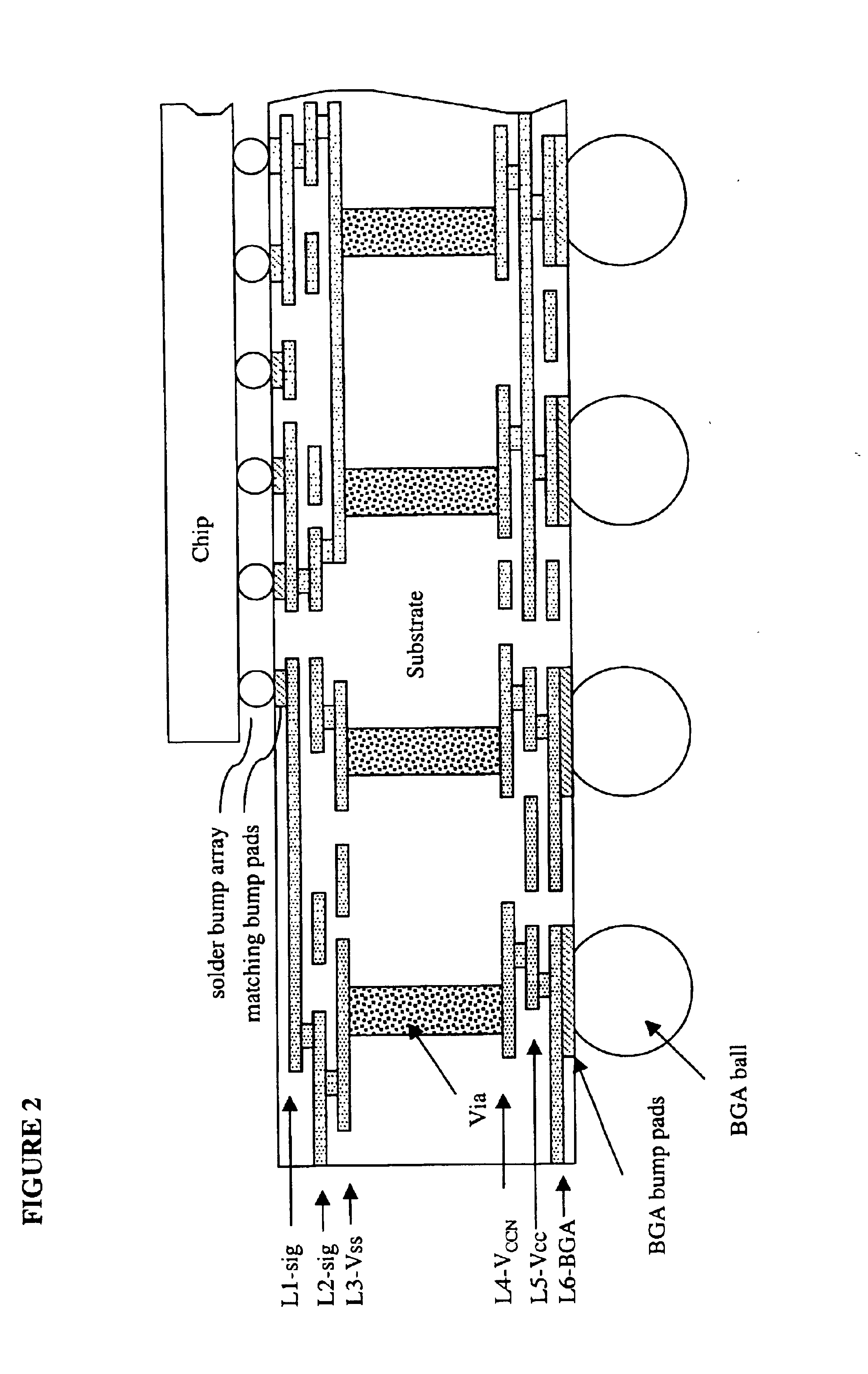
FIG. 3A shows a top view of a flip chip package 300, according to one embodiment of the present invention. Package 300 comprises an IC chip 310 placed on a packaging substrate 320, both being made transparent in FIG. 3A to show some of the routing lines in the package. In one embodiment of the present invention, the packaging substrate 320 has a first side with an array of bump pads (not shown) for bonding with the IC chip 310, and a second side with an array of BGA pads 322 for attaching a grid array of solder balls. The packaging substrate 320 also includes multiple layers of metal routing lines, at least one layer of organic dielectric film separating adjacent layers of metal lines, and a plurality of vias 324 providing connections between different layers of metal lines. The vias and metal routing lines provide electrical connections between the IC chip and the ball grid array. For ease of illustration, only a BGA land layer routing lines 326 are shown in FIG. 3A. The BGA land l...


PUM


Abstract

The present invention includes a semiconductor package and a method of making the semiconductor package. The semiconductor package comprises an IC chip and a substrate, wherein part of the substrate routing such as substrate level trace routing is placed on the IC chip using post-passivation thick metal process at wafer level.

Description

The present invention relates generally to semiconductor packaging technology, and particularly to flip chip packaging technology.BACKGROUND OF THE INVENTIONFlip chip packaging technology has found wide-spread use because of its advantage in size, performance, flexibility, reliability and cost over other packaging methods. Flip chip packaging employs direct electrical connection of face-down integrated circuit (IC) chips onto substrates, circuit boards, or carriers, by means of conductive bumps on the chip bond pads, replacing older wire bonding technology where face-up chips sit on substrates with wire connection to each bond pad. Many of the flip chip bumping techniques developed in recent years have focused on realizing bumps or solderable metallizations directly on the peripheral bond pads of a semiconductor chip. Solder bumping by screen printing solder paste can be used for chip I / O pitches down to 200 micron. However, with increasing IC complexity, the IC pin count has also i...

Claims


Application Information

Patent Timeline
Patent Type & Authority Patents(United States)
IPC IPC(8): H01L29/66H01L29/72H01L23/31H01L23/498H01L23/525
CPCH01L23/3114H01L23/49838H01L23/525H01L23/49822H01L2224/16235H01L2224/16H01L2924/01078H01L2924/01079H01L2924/15174H01L2924/15311H01L2924/0002H01L2224/0401H01L2224/13022H01L2224/05571H01L2224/05008H01L2924/00012H01L2224/05552H01L2224/023H01L2924/0001
Inventor HOOL, VINCENTLONG, JON
Owner ALTERA CORP
Why Eureka
Try Eureka