Windowing circuit for aligning data and clock signals

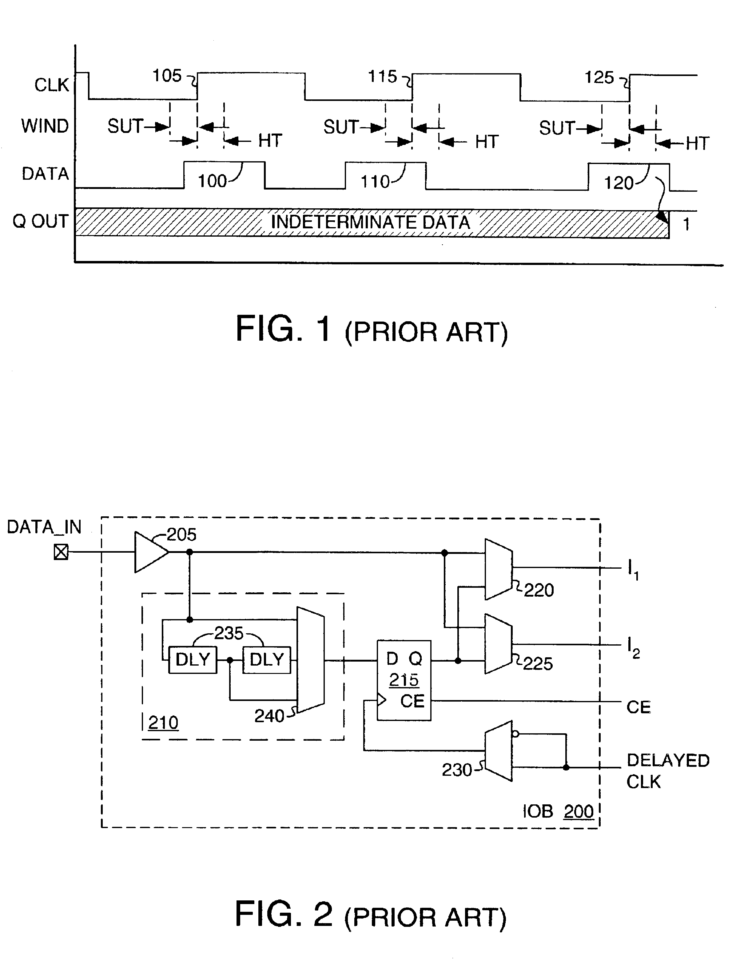
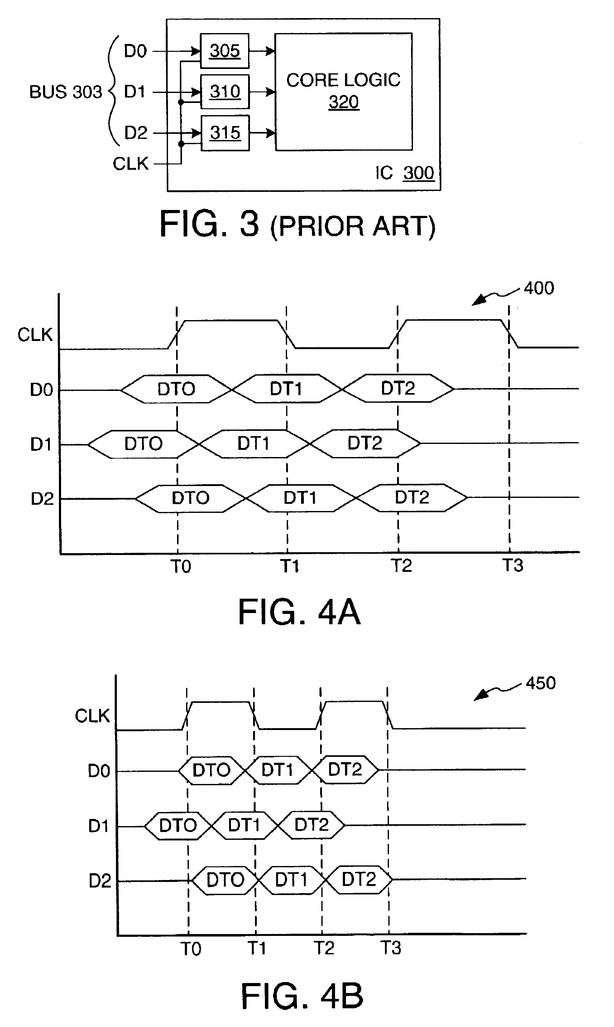
a clock signal and window circuit technology, applied in the field of integrated circuits, can solve the problems of difficult to avoid set-up and hold-time problems, circuit b>300/b> latching incorrect data, and unnecessarily limit the maximum operating frequency of iob b>200/, etc., and achieve precise per-bit data alignment

Inactive Publication Date: 2005-03-08
XILINX INC
View PDF14 Cites 51 Cited by
  • Summary
  • Abstract
  • Description
  • Claims
  • Application Information

AI Technical Summary

Problems solved by technology

It can be difficult, however, to avoid set-up and hold-time problems for sequential storage elements that communicate with data sources external to the chip.
The resulting set-up times work well for relatively low-frequency signals, but unnecessarily limit the maximum operating frequency of IOB 200.
The timing differences between the respective data and clock signals are the same as in FIG. 4A, but the shorter period of the clock and resultant reduced data windows cause circuit 300 to latch incorrect data.
As is apparent from this illustration, the effects of timing errors grow more problematic with increased clock frequency.
This problem is growing ever more severe as new integrated circuits send and receive data at ever-greater speeds to compete in markets where speed performance is paramount.
Nevertheless, even minor differences in signal-propagation delay between different bits sampled on the same clock edge can introduce undesirable errors.

Method used


Image

  • Windowing circuit for aligning data and clock signals
  • Windowing circuit for aligning data and clock signals
  • Windowing circuit for aligning data and clock signals

Examples


Embodiment Construction

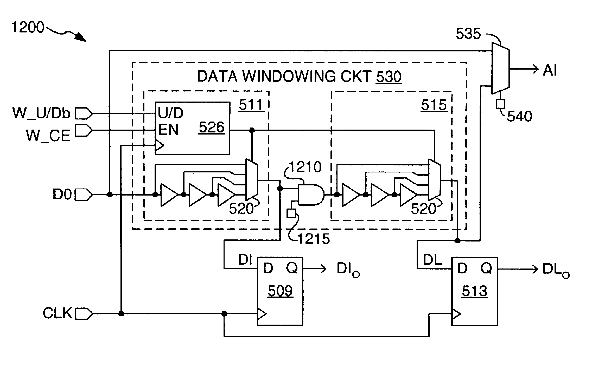
FIG. 5 depicts a data alignment circuit 500 adapted in accordance with one embodiment of the invention to precisely align a data signal on a data input node D0 with a clock signal on a clock input node CLK. In one embodiment, alignment circuit 500 is a portion of an input / output block of a field-programmable gate array (FPGA), or some other type of programmable logic device. Alignment circuit 500 includes three sequential storage elements, each of which includes a data terminal connected to data input node D0. The first sequential storage element 505 connects to data input node D0 via a first direct signal path that includes a first adjustable delay circuit 507; the second sequential storage element 509 includes a second d at a terminal connected to input node D0 via a second direct signal path that includes a second adjustable delay circuit 511 and the first delay circuit 507; and the third sequential storage element 513 connects to data input node D0 via a third direct path that i...


PUM


Abstract

Described are circuits and methods for aligning data and clock signals. Circuits in accordance with some embodiments separate incoming data into three differently timed data signals: an early signal, an intermediate signal, and a late signal. The timing of the three data signals can be collectively moved with respect to the clock signal. In addition, the temporal spacing between the three signals can be adjusted so that the early and late signals define a window encompassing the intermediate signal. The three signals are aligned with respect to the clock edge to center the intermediate data signal on the clock edge. The early and late signals can be monitored to identify changes in the relative timing of the clock and data signals. Some embodiments automatically alter the timing of the data and / or clock signals to keep the intermediate data signal centered on the clock edge.

Description

FIELD OF THE INVENTIONThis application relates to integrated circuits, particularly to timing of data transfer between logic elements.BACKGROUND“Set-up time” and “hold time” together describe the timing requirements on the data input of a sequential logic element, such as a flip-flop or register, with respect to a clock input. The set-up and hold times define a temporal window during which data must be stable to guarantee predictable performance over a full range of operating conditions and manufacturing tolerances. The set-up time SUT is the length of time that data must be available and stable on the input terminal of a storage element before arrival of a clock edge for the data to be captured by the storage element; the hold time HT is the length of time that the data must remain stable after the arrival of the clock edge.FIG. 1 (prior art) depicts three clock-to-data timing scenarios that illustrate the relationships between set-up time, hold time, and clock edges for a given fl...

Claims


Application Information

Patent Timeline
Patent Type & Authority Patents(United States)
IPC IPC(8): G06F1/02G06F1/025H03K19/177H03K5/135H04L7/00
CPCG06F1/025H03K5/135H03K19/1774H04L7/0037H03K19/17764H04L7/0004H04L7/0041
Inventor BAUER, TREVOR J.YOUNG, STEVEN P.EBELING, CHRISTOPHER D.BERGENDAHL, JASON R.BEHIEL, ARTHUR J.
Owner XILINX INC
Why Eureka
Try Eureka