Charge pump stage with body effect minimization

Inactive Publication Date: 2005-03-08
SAIFUN SEMICON
View PDF121 Cites 17 Cited by
  • Summary
  • Abstract
  • Description
  • Claims
  • Application Information

AI Technical Summary

Benefits of technology

The present invention provides a novel charge pump stage for pumping h

Problems solved by technology

However, in positive charge pumps there can be a significant loss of energy in the latter pump stages due to the “body effect”.
This reduces the efficiency of the charge pump, because, the voltage gain of each stage decreases, which means that a higher number of stages is necessary for generating a given voltage.
However, in the prior art, this entails certain risks.
For example, if the bulk voltage is raised above the source or drain voltage, then parasitic bipolar transi

Method used


Image

  • Charge pump stage with body effect minimization
  • Charge pump stage with body effect minimization
  • Charge pump stage with body effect minimization

Examples


Embodiment Construction

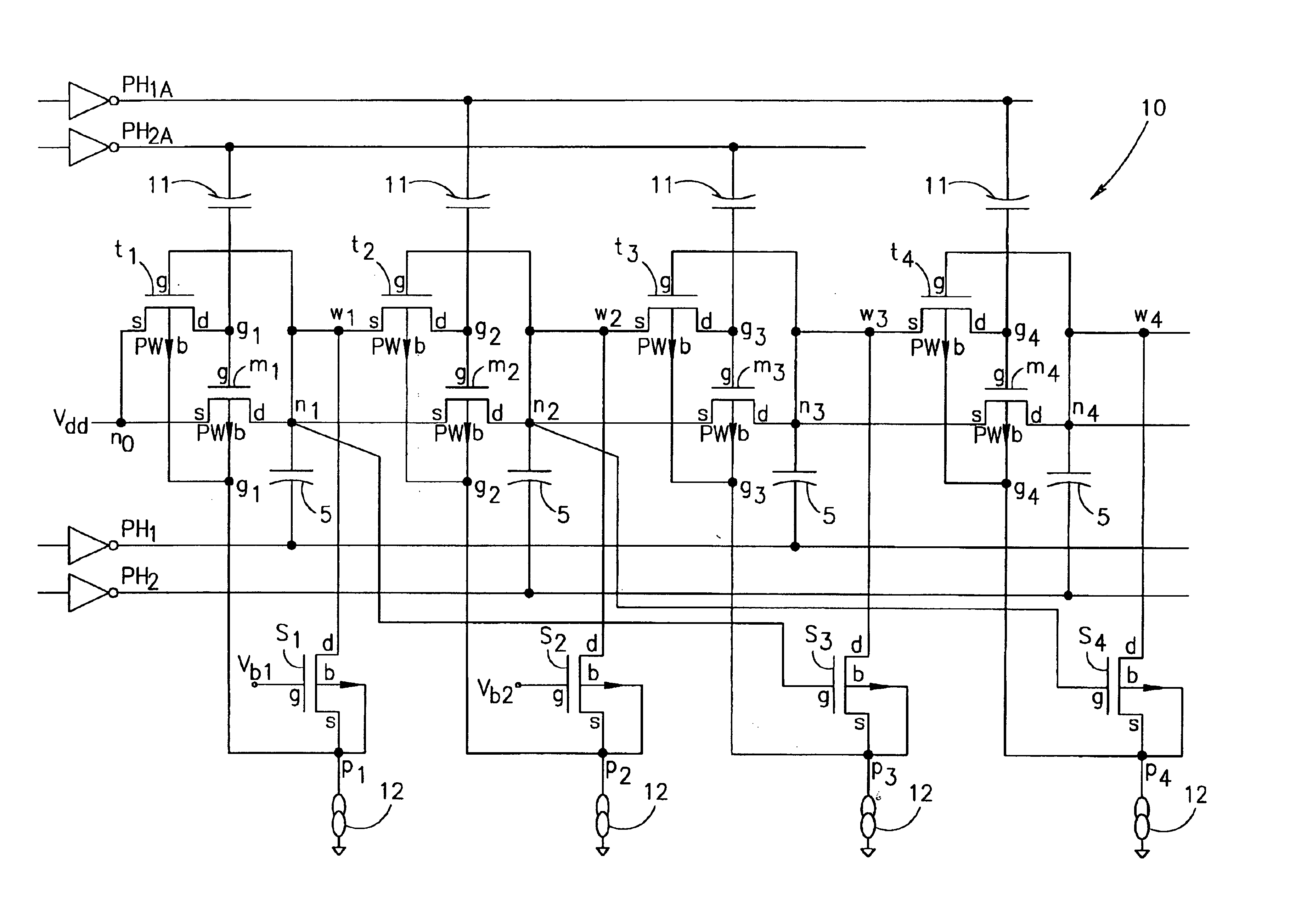
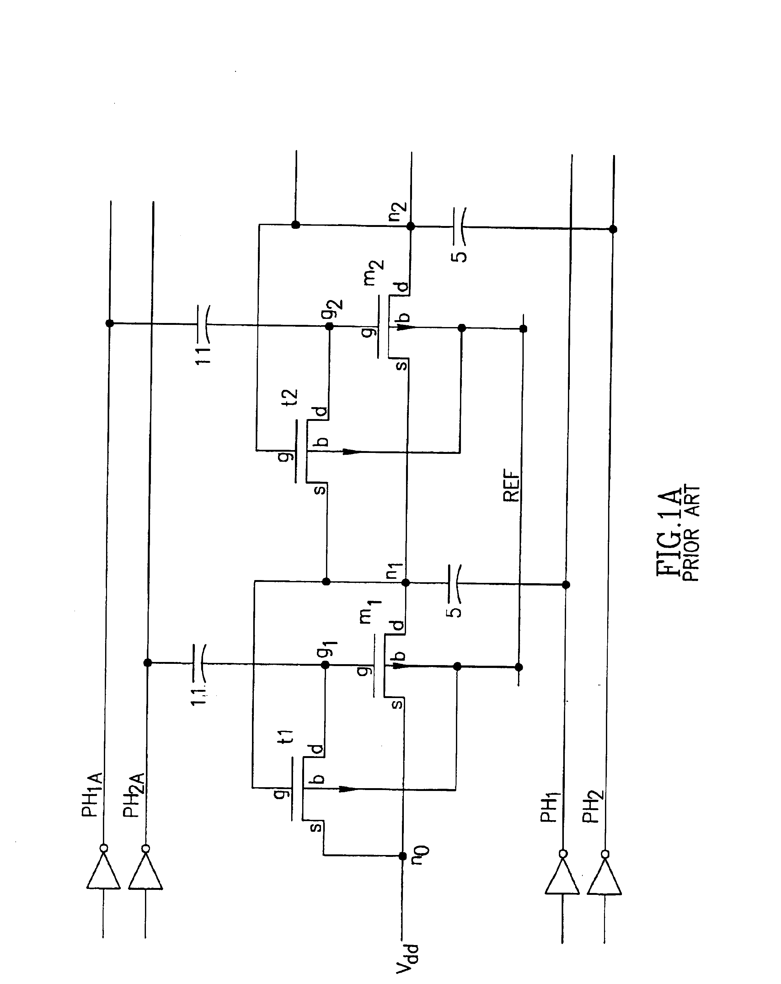
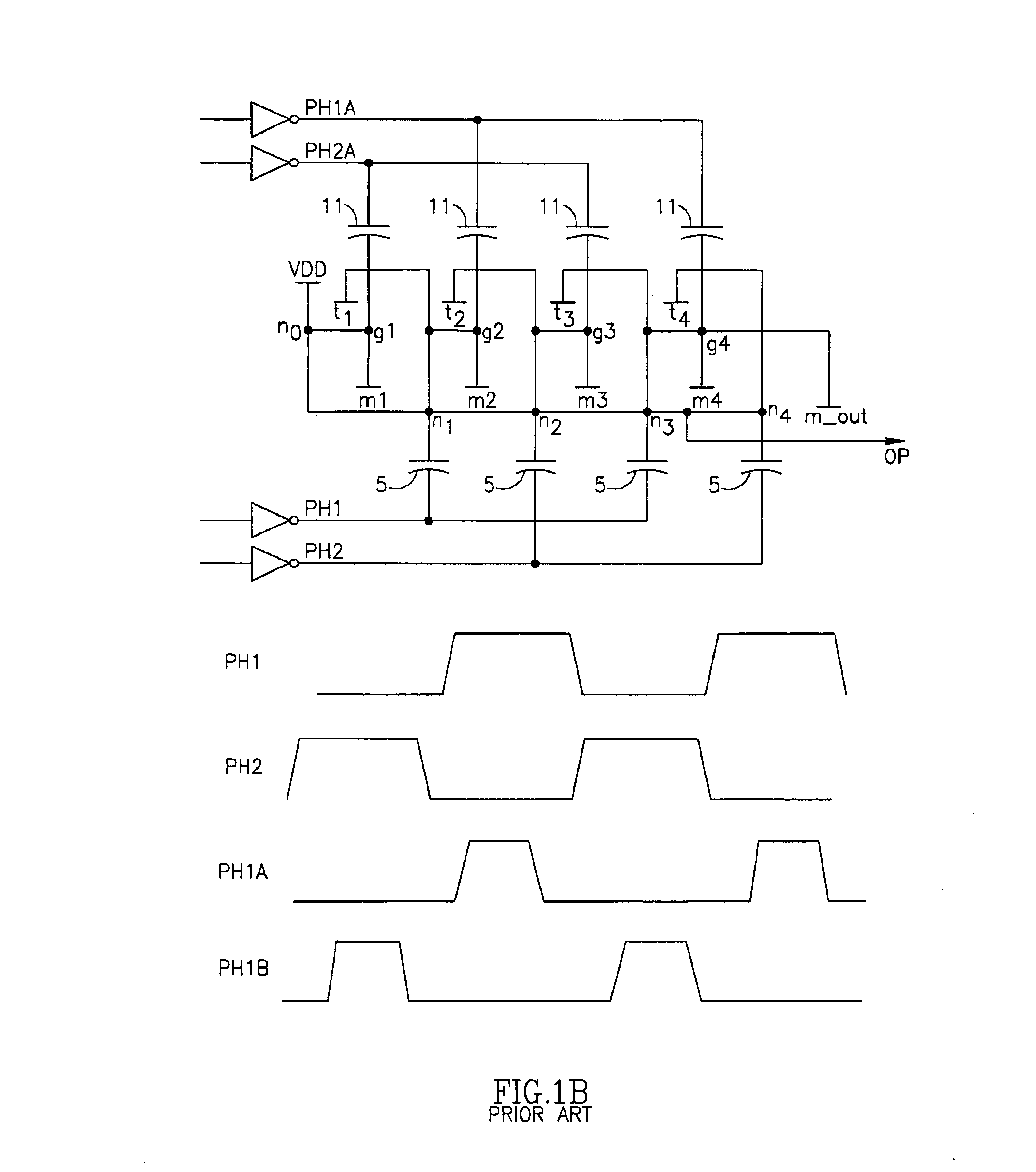
The charge transfer transistors of the present invention are preferably NMOS transistors that have a P-well (PW) isolated from a P-substrate of the integrated circuit (IC), as is now described. This allows independent biasing of the specific NMOS transistor's bulk with respect to the substrate of the IC, which is preferably always grounded.

One way of isolating the P-well from the P-substrate is illustrated in FIG. 4, to which reference is now made. In this embodiment, each charge transfer transistor is a triple-well NMOS transistor 14. Transistor 14 includes a P-well isolated from a P-substrate by an N-well. Two n+ regions are preferably formed in the P-well for connecting to the source and drain. A p+ region is preferably formed in the P-well for connecting to the bulk. An n+ region is preferably formed in the N-well, which is connected to a voltage equal to or higher than p+.

Other transistor architectures may be used to carry out the invention other than triple-well technology. Fo...


PUM


Abstract

A method for operating a charge pump, the method including biasing a bulk of a charge pump stage so as to reduce body effect without forward biasing diodes of the charge pump stage.

Description

FIELD OF THE INVENTIONThe present invention relates generally to charge pumps for boosting voltages in microelectronic circuitry, and particularly to a charge pump stage architecture with body effect minimization.BACKGROUND OF THE INVENTIONNon-volatile memory arrays, such as erasable, programmable read only memory (EPROM) or flash memory arrays, or electrically erasable, programmable read only memory (EEPROM) arrays, require high positive or negative voltages to program and erase memory cells of the array. Typically, these voltages are higher than the voltage supplied (Vdd). Charge pumps are generally used to boost on-chip voltages above the supply voltage Vdd to reach the voltages required for programming or erasing.A charge pump typically comprises cascaded stages that progressively boost the voltage to higher levels. The charge pump functions by progressively storing more charge on a capacitor which is part of a capacitor-diode combination, with several such stages being placed t...

Claims


Application Information

Patent Timeline
IPC IPC(8): H02M3/04H02M3/07
CPCH02M3/073H02M2003/078H02M3/078
Inventor SHOR, JOSEPH S.MAAYAN, EDUARDOPOLANSKY, YAN
Owner SAIFUN SEMICON
Why Eureka
Try Eureka