High voltage reset method for increasing the dynamic range of a CMOS image sensor

a high-voltage reset and image sensor technology, applied in the field of cmos image sensors, can solve the problems of reducing the dynamic range of image sensors using cmos chips, ccd image sensors are much more expensive to manufacture than cmos image sensors, and the dynamic range of image sensors is much less. achieve the effect of increasing the dynamic range of an image sensor and higher voltage level

Inactive Publication Date: 2005-03-08
OMNIVISION TECH INC
View PDF7 Cites 48 Cited by
  • Summary
  • Abstract
  • Description
  • Claims
  • Application Information

AI Technical Summary

Benefits of technology

In yet another embodiment of the invention, a circuit for increasing a dynamic range of an image sensor is provided. The circuit includes a means for generating a high supply voltage, a means for receiving a reset signal and a means for generating a high reset signal based on the reset signal and the high supply voltage. The high supply voltage has a higher voltage level than a maximum supply voltage of an...

Problems solved by technology

However, CCD image sensors are much more expensive to manufacture than CMOS image sensors.
While the increased processing power and processing speeds are advantageous to many of the technologies using CMOS chips (i.e., micr...

Method used


Image

  • High voltage reset method for increasing the dynamic range of a CMOS image sensor
  • High voltage reset method for increasing the dynamic range of a CMOS image sensor
  • High voltage reset method for increasing the dynamic range of a CMOS image sensor

Examples


Embodiment Construction

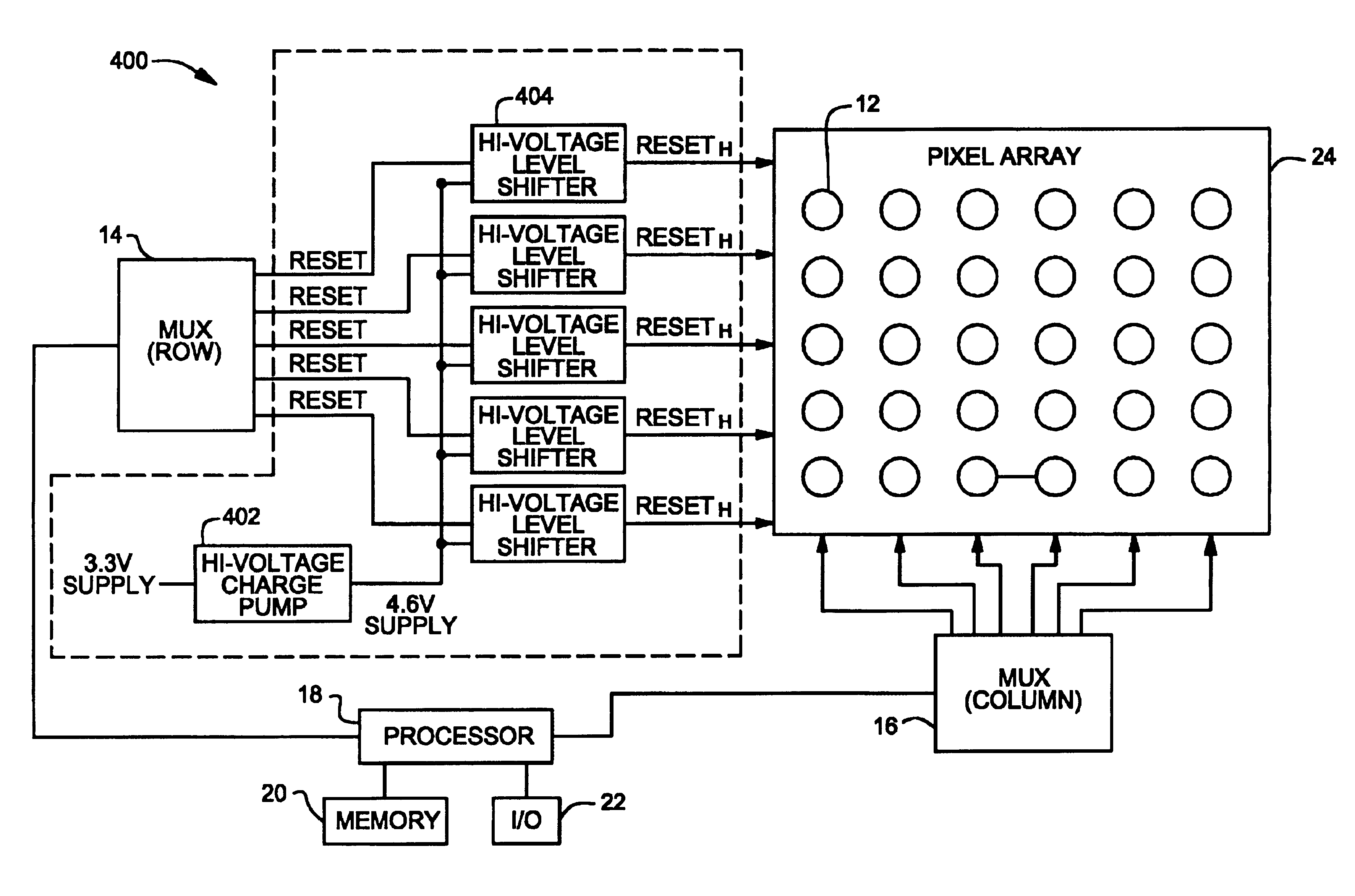
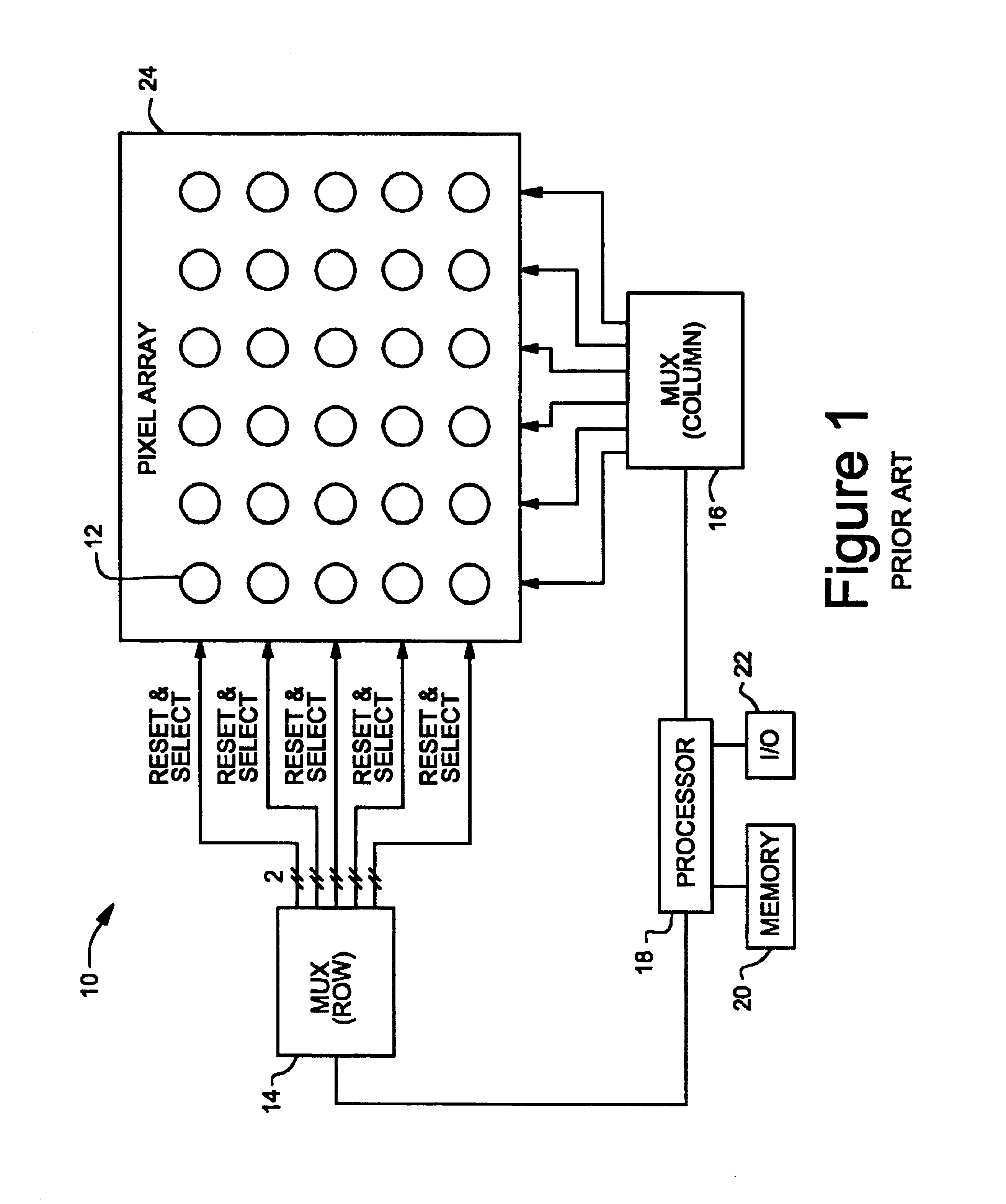
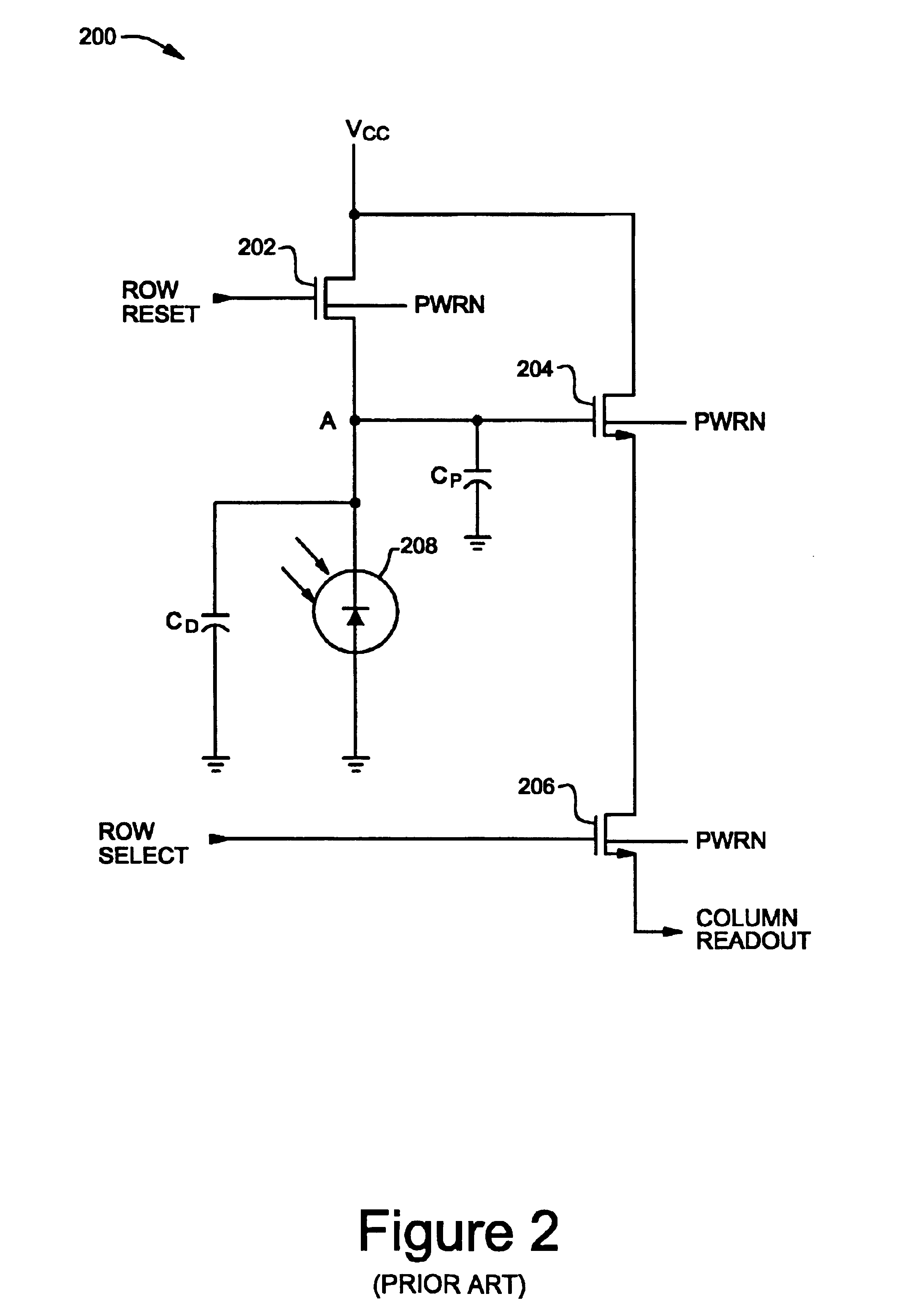
Briefly described, the present invention is directed at a system and method for increasing the dynamic range of CMOS image sensors designed with a thin gate oxide layer. As mentioned above, the fabrication process for CMOS chips continues to progress towards smaller dimensions. These smaller dimensions require smaller maximum supply voltages which decrease the ability of a pixel ell to detect contrast details in both bright and dark regions of a sensed image (i.e., the dynamic range). For a pixel cell with a relatively low dynamic range, either the dark regions of the sensed image will be underexposed or the bright regions will be overexposed. This phenomenon is best described using a conventional CMOS image sensor as illustrated in FIGS. 1-3.

FIG. 1 shows a conventional CMOS image sensor 10, which includes an array 24 of individual pixel cells 12 arranged in columns and rows. A processor 18 is coupled to an input / output interface 22, a memory 20 and a row multiplexer 14, which is em...


PUM


Abstract

A circuit and method for increasing the dynamic range of CMOS image sensors designed with a thin gate oxide layer. The circuit includes a high voltage supply circuit and a high voltage level shifter circuit. The high voltage supply circuit is configured to supply a voltage to the shifter circuit. The voltage has a voltage level higher than the maximum supply voltage of the associated fabrication process. The shifter circuit is configured to output a high reset signal based on a reset signal generated to reset a pixel circuit of a pixel array. Instead of the reset signal, the high reset signal is coupled to a gate of the reset transistor in the pixel circuit. The high reset signal allows the reset transistor to maintain a gate to source potential less than the maximum supply voltage even when the high reset signal is greater than the maximum supply voltage.

Description

FIELD OF THE INVENTIONThe present invention relates generally to CMOS image sensors, and more particularly to integrated CMOS transistor logic circuits for increasing the dynamic range of the CMOS image sensor.BACKGROUND OF THE INVENTIONDigital cameras have become extremely common lately. There are two prevalent technologies used in digital cameras: charge-coupled device (CCD) image sensors and complimentary metal-oxide semiconductor (CMOS) image sensors. Both of these image sensors depend on the photovoltaic response resulting when silicon is exposed to light. The photons in the light have energy that breaks covalent bonds in the silicon. The electrons that are released when the covalent bonds are broken result in a photocurrent when an electric field carries the electrons away. A photodiode may collect the photocharge carried in the photocurrent, thus providing a detectable signal. The dynamic range of the image sensor is the ratio of the largest detectable signal to the smallest ...

Claims


Application Information

Patent Timeline
IPC IPC(8): H04N5/335H04N5/355H04N5/374H04N5/376
CPCH04N3/155H04N3/1512H04N25/76H04N25/77
Inventor KINDT, WILLEM J.PHAN, CHRISTINA P.GUPTA, SHIVANI
Owner OMNIVISION TECH INC
Why Eureka
Try Eureka