Organic electroluminescence device emitting white light
- Summary
- Abstract
- Description
- Claims
- Application Information
AI Technical Summary
Benefits of technology
Problems solved by technology
Method used
Image
Examples
example 1
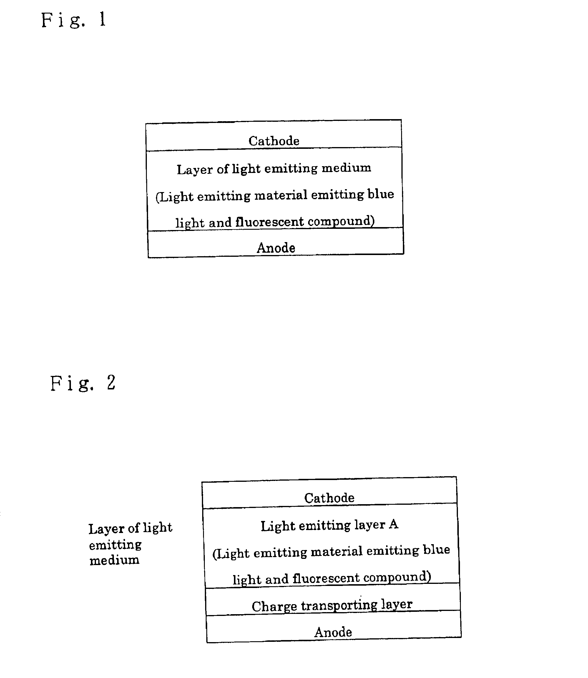
Preparation of an organic EL device (An example of the first construction: the fluoranthene skeleton structure)
A glass substrate of 25 mm×75 mm×1.1 mm thickness having a transparent electrode line of ITO (In—Sn—O) (manufactured by GEOMATEC Company) was cleaned with isopropyl alcohol for 5 minutes under application of ultrasonic wave and treated by the UV ozone cleaning for 30 minutes. The cleaned glass substrate having a transparent electrode line was attached to a substrate holder in a vacuum vapor deposition apparatus. On the face of the substrate on which the transparent electrode line was disposed, a film of N,N′-bis(N,N-diphenyl-4-aminphenyl)-N,N-diphenyl-4,4′-diamino-1,1′-biphenyl (a TPD232 film) having a thickness of 60 nm was formed in a manner such that the film covered the transparent electrode line. The TPD232 film worked as the hole injecting layer. Then, a film of 4,4′-bis[N-(1-naphthyl)-N-phenylamino]biphenyl (an NPD film) having a thickness of 20 nm was formed on the ...
example 2
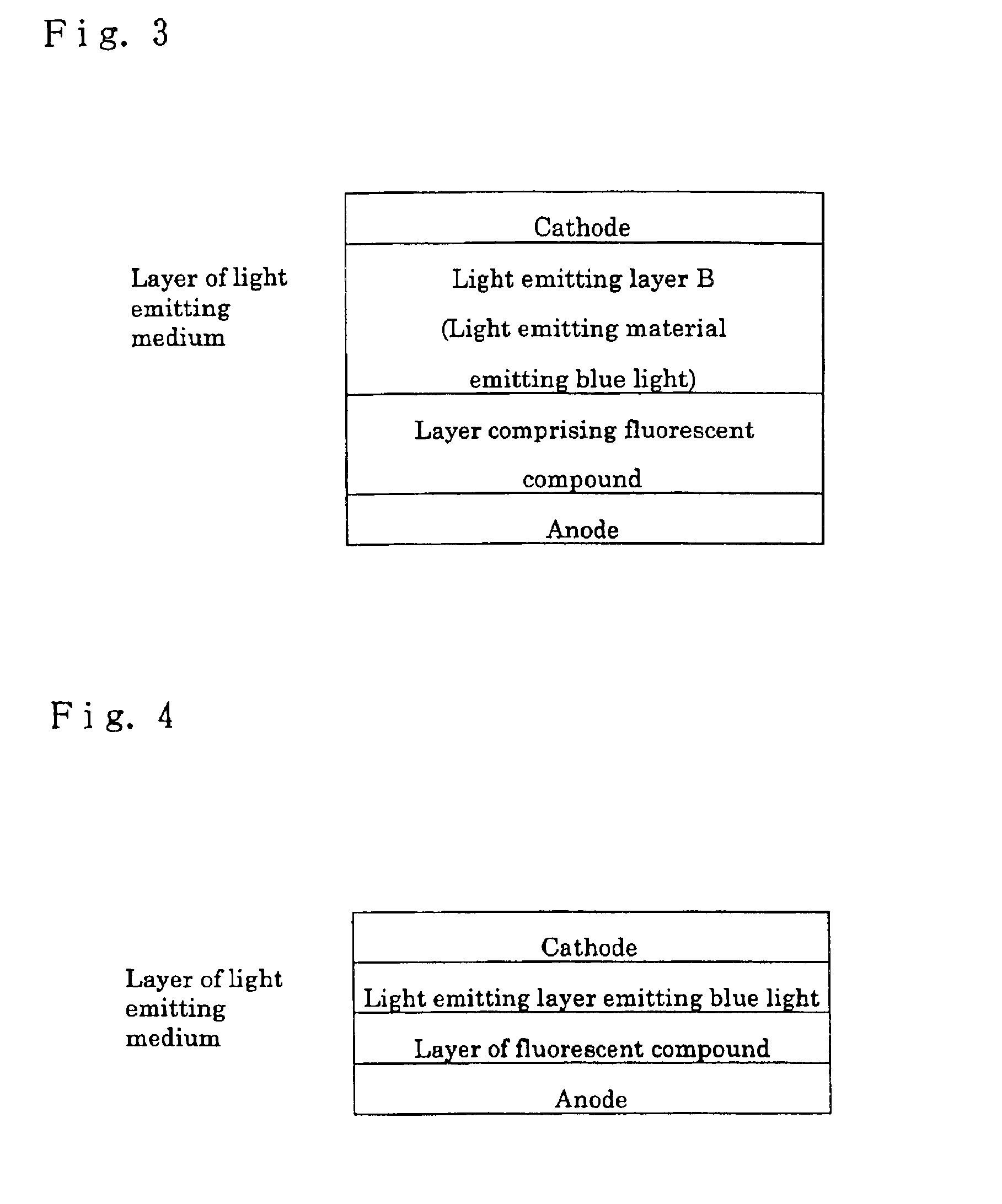
Preparation of an organic EL device (An example of the second construction: the fluoranthene skeleton structure)
A glass substrate of 25 mm×75 mm×1.1 mm thickness having a transparent electrode line of ITO (In—Sn—O) (manufactured by GEOMATEC Company) was cleaned with isopropyl alcohol for 5 minutes under application of ultrasonic wave and treated by the UV ozone cleaning for 30 minutes. The cleaned glass substrate having a transparent electrode line was attached to a substrate holder in a vacuum vapor deposition apparatus. On the face of the substrate on which the transparent electrode line was disposed, a TPD232 film having a thickness of 60 nm was formed in a manner such that the film covered the transparent electrode line. The TPD232 film worked as the hole injecting layer. Then, an NPD film having a thickness of 20 nm was formed on the TPD232 film. When the NPD film was formed, the fluorescent compound described above (E1) was added in an amount such that the amounts by weight of...
example 3
Preparation of an organic EL device (An example of the third construction: the fluoranthene skeleton structure)
A glass substrate of 25 mm×75 mm×1.1 mm thickness having a transparent electrode line of ITO (In-Sn-O) (manufactured by GEOMATEC Company) was cleaned with isopropyl alcohol for 5 minutes under application of ultrasonic wave and treated by the UV ozone cleaning for 30 minutes. The cleaned glass substrate having a transparent electrode line was attached to a substrate holder in a vacuum vapor deposition apparatus. On the face of the substrate on which the transparent electrode line was disposed, a TPD232 film having a thickness of 60 nm was formed in a manner such that the film covered the transparent electrode line. The TPD232 film worked as the hole injecting layer. Then, an NPD film having a thickness of 20 nm was formed on the TPD232 film. The NPD film worked as the hole transporting layer. On the NPD film, the fluorescent compound (E1) described above was vapor deposited...
PUM
| Property | Measurement | Unit |
|---|---|---|
| Wavelength | aaaaa | aaaaa |
| Structure | aaaaa | aaaaa |
| Fluorescence | aaaaa | aaaaa |
Abstract
Description
Claims
Application Information


