Switch mode power supply and driving method for efficient RF amplification

a technology of rf amplification and power supply, applied in the direction of logic circuit coupling/interface arrangement, pulse technique, instruments, etc., can solve the problems of increasing turn-off time, and achieve the effect of reducing turn-off time, reducing power consumption, and reducing power consumption

Inactive Publication Date: 2005-03-15
III HLDG 12 LLC
View PDF8 Cites 6 Cited by
  • Summary
  • Abstract
  • Description
  • Claims
  • Application Information

AI Technical Summary

Benefits of technology

The present invention, generally speaking, provides a power-efficient method of driving a switch mode power supply at higher frequencies than those typically attainable in the prior art. In an exemplary embodiment, driver transistors exhibit gate capacitance, which is exploited by charging the gate capacitance using a pulse signal and thereafter allowing the gate capacitance to discharge. With the gate capacitance charged, the driver transistor remains on for the desired period of time even without a drive signal being continuously applied, thus conserving power. In essence, the gate capacitance is exploited in the manner of a memory cell. Furthermore, at higher-frequency operation, instead of the gate capacitance being fully charged, leading to increased turn-off time, the gate capacitance is only partially charged, allowing for quicker turn around. The envelope-following capability of the switch mode power supply, in telecommunications applications, is therefore increased. In accordance with another aspect of the invention, in RF amplification circuit having a phase path and a magnitude path, an amplifier is provided having at least a final stage, the amplifier having an RF input coupled to the phase path; and a switch mode power supply is coupled to an operational voltage and to a power supply input terminal of the amplifier. The switch mode power supply includes a transistor switch, a driver circuit for driving the transistor switch, and a controller, the controller causing the driver circuit to operate in charge transfer mode in which a pulse of short duration relative to a duty cycle of the switch mode power supply is used to turn on the transistor switch.

Problems solved by technology

Furthermore, at higher-frequency operation, instead of the gate capacitance being fully charged, leading to increased turn-off time, the gate capacitance is only partially charged, allowing for quicker turn around.

Method used


Image

  • Switch mode power supply and driving method for efficient RF amplification
  • Switch mode power supply and driving method for efficient RF amplification
  • Switch mode power supply and driving method for efficient RF amplification

Examples


Embodiment Construction

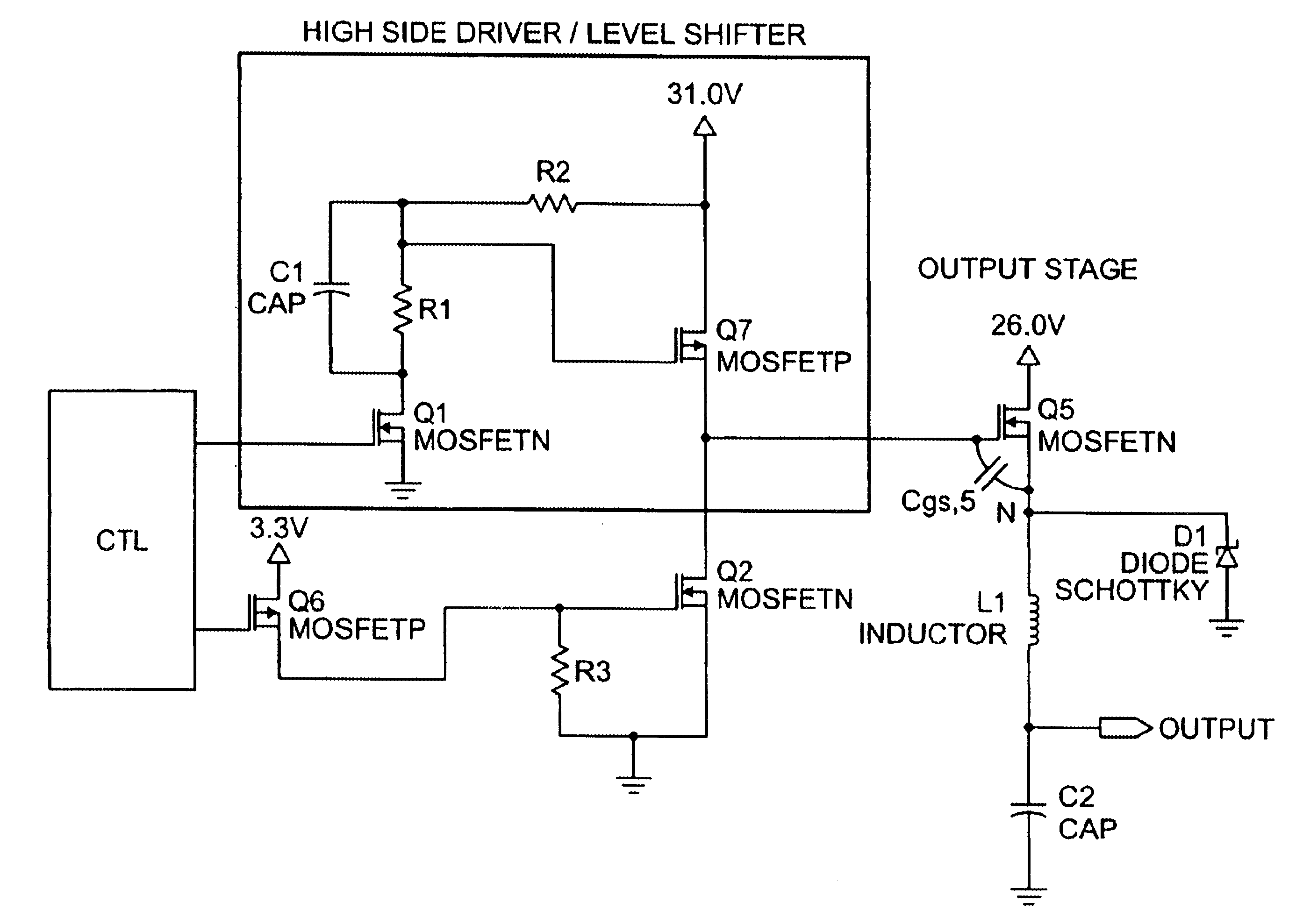
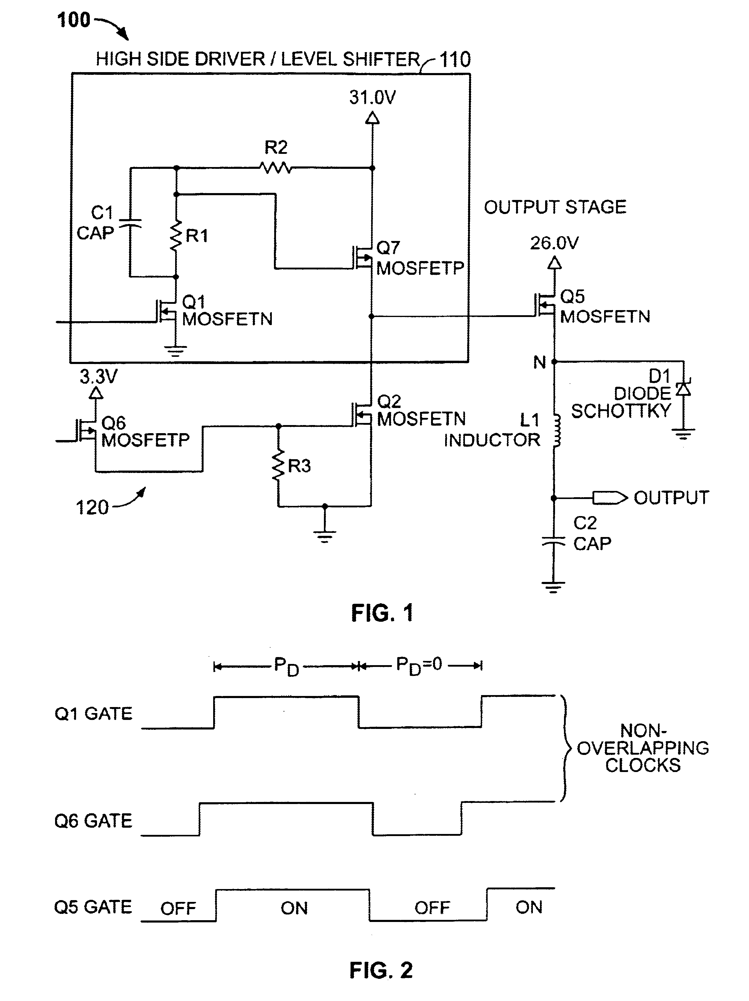
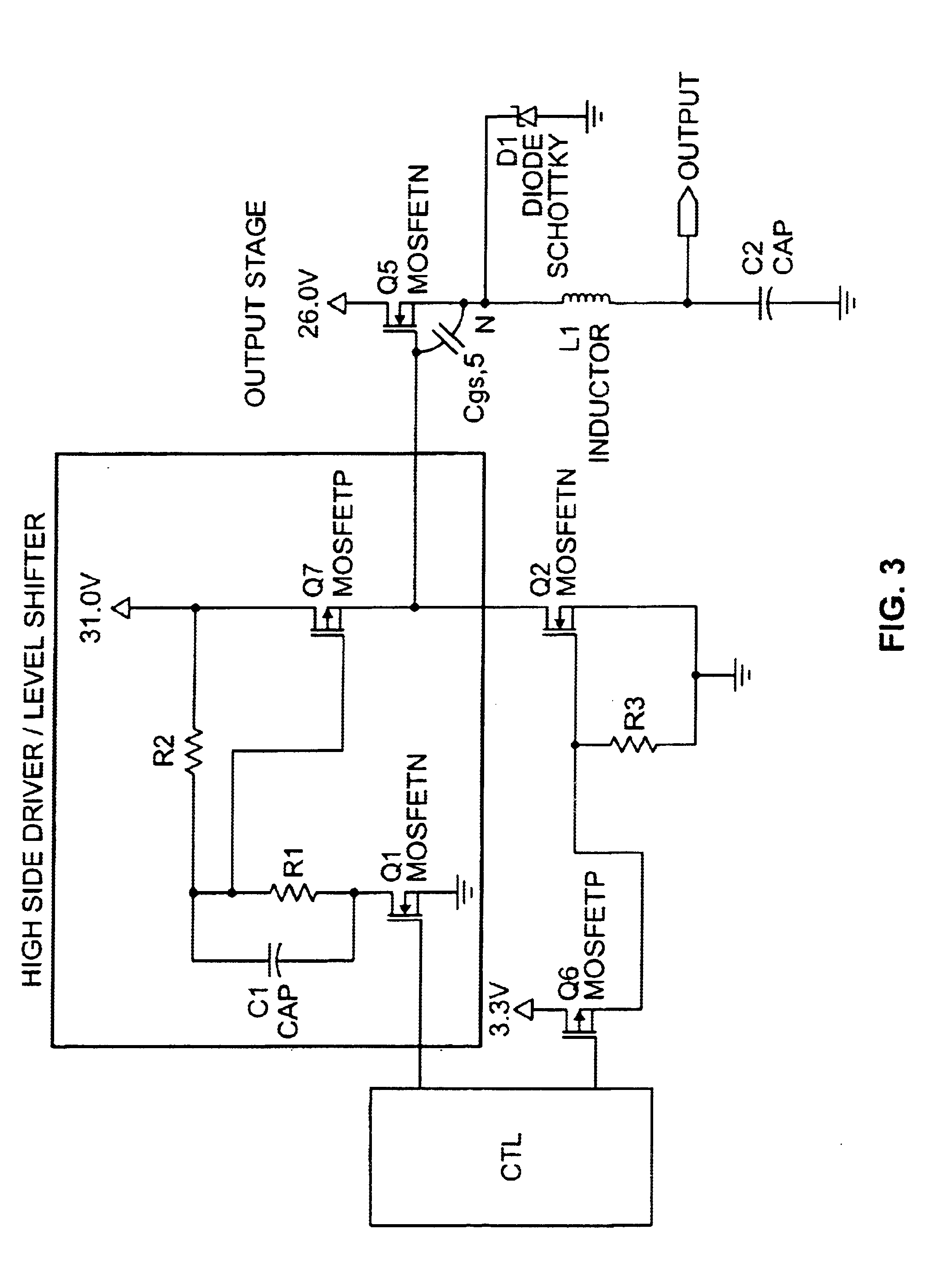
Referring now to FIG. 3 and FIG. 4, a diagram is shown of a switch mode power supply in which a parasitic gate capacitance Cgs,5 is used to advantage (FIG. 3), together with a waveform diagram (FIG. 4) illustrating the method of the invention in an exemplary embodiment thereof. To reduce power consumption in the resistive divider network of the circuit of FIG. 1, the time for which the gate electrode of the transistor Q1 is held high is minimized. In particular, the gate electrode of the transistor Q1 is pulsed high for a length of time calculated to charge the parasitic gate capacitance of the transistor Q5 and maintain the transistor in the ON state for up to the maximum expected positive portion of duty cycle.

At the point in time when the transistor Q5 is to be turned off, the gate electrode of the transistor Q6 is pulsed low, discharging the parasitic gate capacitance of the transistor Q5 and causing it to turn off.

Referring still to FIG. 4, the driver circuit alternates between...


PUM


Abstract

The present invention, generally speaking, provides a power-efficient method of driving a switch mode power supply at higher frequencies than those typically attainable in the prior art. In an exemplary embodiment, driver transistors exhibit gate capacitance, which is exploited by charging the gate capacitance using a pulse signal and thereafter allowing the gate capacitance to discharge. With the gate capacitance charged, the driver transistor remains on for the desired period of time even without a drive signal being continuously applied, thus conserving power. In essence, the gate capacitance is exploited in the manner of a memory cell. Furthermore, at higher-frequency operation, instead of the gate capacitance being fully charged, leading to increased turn-off time, the gate capacitance is only partially charged, allowing for quicker turn around. The envelope-following capability of the switch mode power supply, in telecommunications applications, is therefore increased. In accordance with another aspect of the invention, in RF amplification circuit having a phase path and a magnitude path, an amplifier is provided having at least a final stage, the amplifier having an RF input coupled to the phase path; and a switch mode power supply is coupled to an operational voltage and to a power supply input terminal of the amplifier. The switch mode power supply includes a transistor switch, a driver circuit for driving the transistor switch, and a controller, the controller causing the driver circuit to operate in charge transfer mode in which a pulse of short duration relative to a duty cycle of the switch mode power supply is used to turn on the transistor switch.

Description

BACKGROUND OF THE INVENTION1. Field of the InventionThe present invention relates to switch mode power supplies and driving methods, particularly for efficient RF amplification, as well as amplifier structures using the same.2. State of the ArtAs is well-known, the efficiency of power amplifiers such as those used in wireless telecommunications can be increased substantially using a variable power supply instead of a fixed power supply. In this application, as well as a wide variety of other applications, a switch mode power supply may be used to efficiently perform DC-to-DC conversion from a fixed DC power supply input to a variable supply output.One example of a known switch mode power supply (in particular a buck converter) and associated driver circuit is shown in FIG. 1. A transistor switch Q5 (in this instance a N-FET device) is alternately switched ON and OFF in accordance with some duty cycle during an ON portion of which an operational voltage VDD is coupled to an output fi...

Claims


Application Information

Patent Timeline
Patent Type & Authority Patents(United States)
IPC IPC(8): H02M3/155H02M3/04H03F1/02H03K17/0412H03K17/04H02M1/08H03K17/687H03K19/0185
CPCH02M3/155H03K17/04123H03F1/0227
Inventor SILIC, BOJAN
Owner III HLDG 12 LLC
Why Eureka
Try Eureka