Stacked-NMOS-triggered SCR device for ESD-protection

a technology of esd protection and scr device, which is applied in the direction of emergency protective circuit arrangement, emergency protective circuit arrangement for limiting excess voltage/current, and emergency protective circuit arrangement for addressing excess voltage, etc., can solve the problems of gate oxide damage with breakdown voltage, electric shock can melt or otherwise destroy tiny structures in an integrated circuit, and thin gate oxides present challenges

Inactive Publication Date: 2005-03-15
DIODES INC
View PDF10 Cites 53 Cited by
  • Summary
  • Abstract
  • Description
  • Claims
  • Application Information

AI Technical Summary

Problems solved by technology

Relatively small electric shocks can melt or otherwise destroy tiny structures in an integrated circuit (IC).
These thin gate oxides present a challenge since they may be damaged by relatively small voltages.
However, the IC chip with the thin gate oxide may be electrically connected to another chip that drives S-volt signals that could destroy the delicate gate oxides.
Even reduced voltages such as 3.3 volts may damage gate oxides with breakdown voltages of 4 volts, since a 3.3-volt signal is so close to the breakdown limit.
While useful, the extra processing steps for the thicker I / O oxide add cost and are not desirable.
This means a degraded ESD performance is expected in a stacked transistor structure.
The higher breakdown voltage of the larger NPN transistor 22 is undesirable since it allows a larger voltage to occur on the pad during an ESD event.
The larger ESD voltage that occurs before the parasitic NPN transistor turns on can damage the transistors and gate oxides, causing permanent failures from ESD events.
Simply adding a standard ESD structure to the pad can cause reliability failures.
A standard ESD structure with a single transistor to shunt current from the pad to ground or power could have gate-oxide failures due to the full voltage across the one shunt transistor.

Method used


Image

  • Stacked-NMOS-triggered SCR device for ESD-protection
  • Stacked-NMOS-triggered SCR device for ESD-protection
  • Stacked-NMOS-triggered SCR device for ESD-protection

Examples


Embodiment Construction

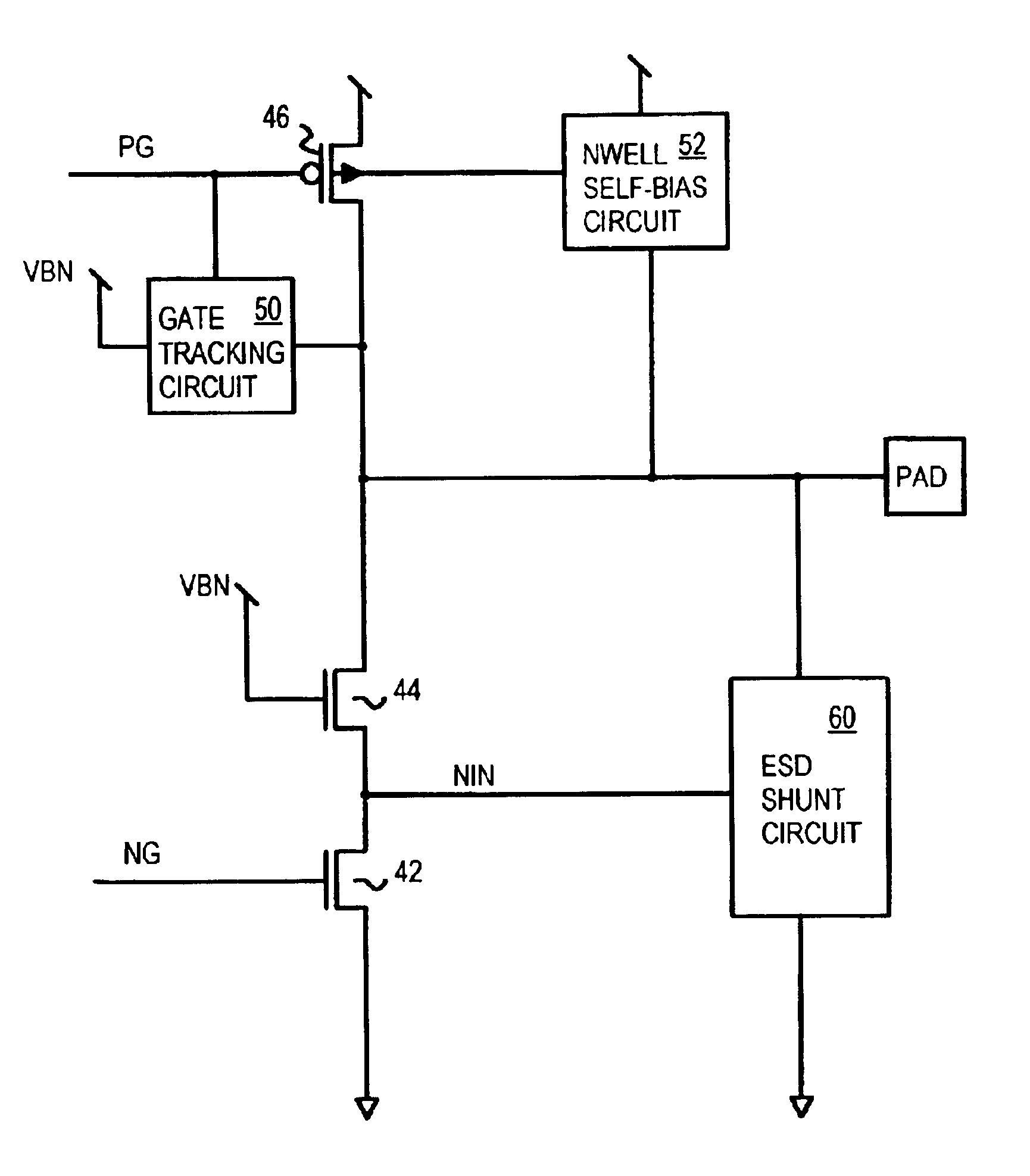
The present invention relates to an improvement in ESD protection circuits. The following description is presented to enable one of ordinary skill in the art to make and use the invention as provided in the context of a particular application and its requirements. Various modifications to the preferred embodiment will be apparent to those with skill in the art, and the general principles defined herein may be applied to other embodiments. Therefore, the present invention is not intended to be limited to the particular embodiments shown and described, but is to be accorded the widest scope consistent with the principles and novel features herein disclosed.

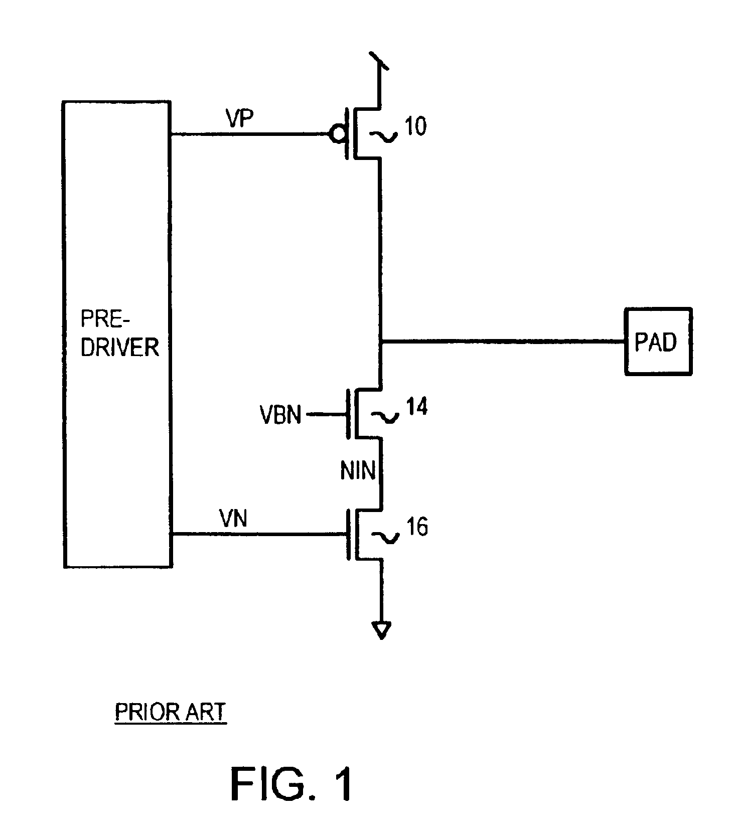
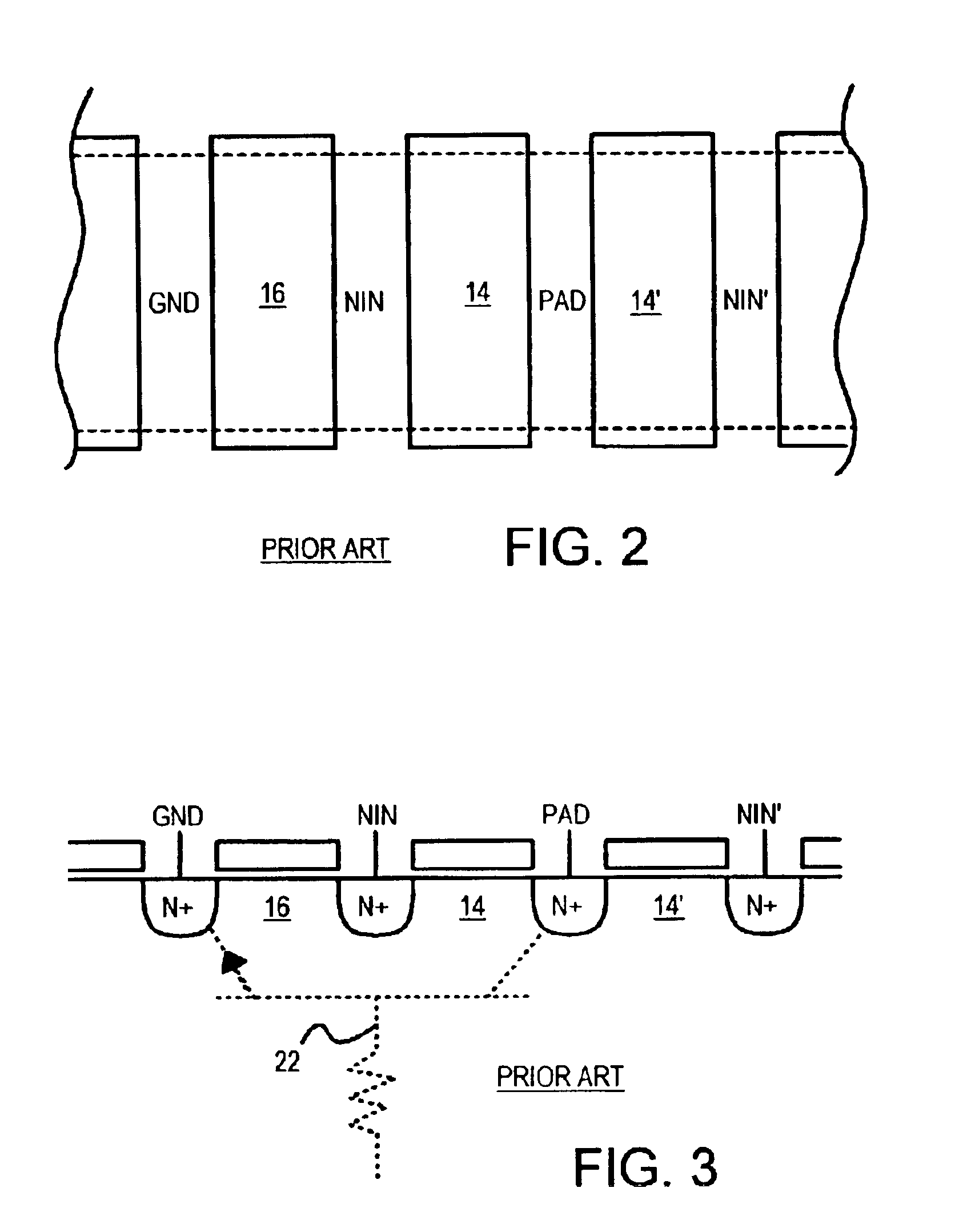
The inventors have realized that the floating intermediate node between two transistors cascaded together increases the breakdown or snapback voltage of the parasitic NPN transistor. The parasitic NPN transistor is harder to turn on, providing less protection during an ESD event, possibly resulting in failures and damage.

The invento...


PUM


Abstract

Transistors with very thin gate oxides are protected against oxide failure by cascading two or more transistors in series between an output pad and ground. The intermediate source / drain node between the two cascaded transistors is usually floating during an ESD test, delaying snapback turn-on of a parasitic lateral NPN transistor. This intermediate node is used to drive the gate of an upper trigger transistor. A lower trigger transistor has a gate node that is charged by the ESD pulse on the pad through a coupling capacitor. When the coupled ESD pulse turns on the trigger transistors, the trigger transistors turn on a silicon-controlled rectifier (SCR) that is integrated with the trigger transistors.

Description

BACKGROUND OF INVENTIONThis invention relates to electro-static-discharge (ESD) protection circuits, and more particularly to cascaded-transistor input-protection devices.Relatively small electric shocks can melt or otherwise destroy tiny structures in an integrated circuit (IC). To reduce such damage, input and output pads of IC chips are typically connected to protection devices specifically designed to shunt electro-static-discharges (ESD). These ESD-protection devices have been effective for semiconductor processes used in the last decade.Processing improvements have continued to reduce the size of IC transistors and the thicknesses of films used to make the transistors. For example, the gate oxide between the silicon substrate and the polysilicon or other gate material has been reduced to as little as 32 angstroms for a process with a minimum gate length of 0.18 micron. These thin gate oxides present a challenge since they may be damaged by relatively small voltages.For example...

Claims


Application Information

Patent Timeline
Patent Type & Authority Patents(United States)
IPC IPC(8): H02H9/00H01L27/02
CPCH01L27/0266H01L27/0262
Inventor TONG, PAUL C. F.KER, MING-DOUXU, PING PING
Owner DIODES INC
Why Eureka
Try Eureka