Magnetic random access memory

Inactive Publication Date: 2005-03-15
SK HYNIX INC
View PDF1 Cites 12 Cited by
  • Summary
  • Abstract
  • Description
  • Claims
  • Application Information

AI Technical Summary

Benefits of technology

Accordingly, in order to overcome the above-described problem, it is an object of the present invention to store two or more data by comb

Problems solved by technology

However, the above-described conventional MRAM has a complicated structure of a cell because a cell includes 1T+1MTJ.
In other words, a process

Method used


Image

  • Magnetic random access memory
  • Magnetic random access memory
  • Magnetic random access memory

Examples


Embodiment Construction

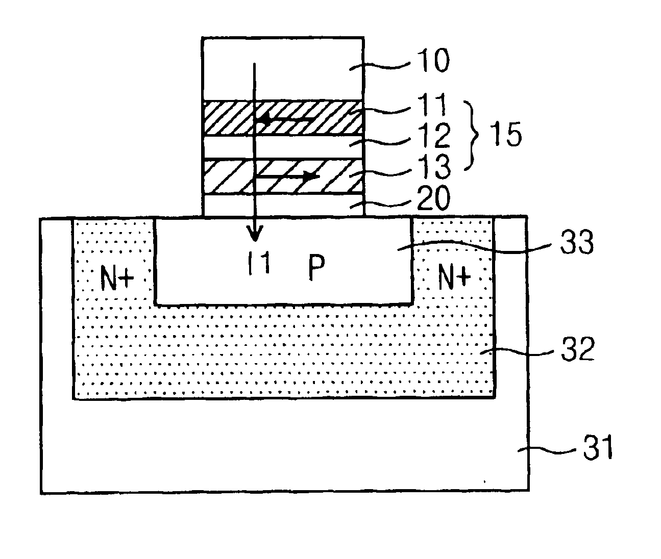
A MRAM of FIGS. 3a and 3b comprises an MTJ 15 deposited on the top portion of a P-type impurity region 33 of a P-N diode device.

A MRAM of the present invention includes an N+ region 32 doped on a semiconductor substrate 31 and a P-N diode comprising a P-type impurity region 33 doped on the line of the N+ region 32. A barrier conductive layer 20 is deposited on the top portion of the P-type impurity region 33. An MTJ is then deposited on the top portion of the barrier conductive layer 20, the MTJ comprising a free ferromagnetic layer 11, a tunnel junction layer 12 and a fixed ferromagnetic layer 13. A word line 10 is formed on the top portion of the MTJ 15.

FIGS. 4a and 4b are cross-sectional diagrams of an MRAM cell in accordance with another preferred embodiment of the present invention.

A MRAM of the present invention include an oxide film 32 and a P-N diode. The oxide film 32 is deposited on a semiconductor substrate 31. The P-N diode comprises an N-type polysilicon 33 deposited on...


PUM


Abstract

The present invention discloses a magnetic random access memory comprising MRAM cell groups connected in series in forms of an NAND. The MRAM cell groups comprise magnetic tunnel junctions between word lines and P-N diodes, and memory cells for reading and writing data. In the present invention, the cell size can be reduced by comprising MRAM cell arrays wherein one or more MRAM cells are connected in series in forms of an NAND.

Description

BACKGROUND OF THE INVENTION1. Field of the InventionThe present invention generally relates to a magnetic random access memory (hereinafter, referred to as “MRAM”), and in particular, to an MRAM comprising a magnetic tunnel junction (hereinafter, referred to as “MTJ”) between a word line and a P-N diode, the MRAM wherein memory cells for storing two or more data are connected in series to each other in a form of an NAND, and data is read / written therein.2. Description of the Prior ArtMost of companies for fabricating semiconductor memory are developing an MRAM using ferromagnetic materials, which is one of the next generation memory devices. An MRAM is a memory form for storing magnetic polarization in the thin film of magnetic materials. In the MRAM, read / write operations are performed by changing magnetic polarization according to the magnetic field generated by combining currents in a bit line and a word line.The above MRAM is comprised of various kinds of cells such as a giant m...

Claims


Application Information

Patent Timeline
IPC IPC(8): G11C11/15G11C11/02H01L21/8246H01L27/105H01L43/08
CPCG11C11/15
Inventor KANG, HEE BOKLEE, GEUN ILKIM, JUNG HWANKYE, HUN WOOKIM, DUCK JUPARK, JE HOON
Owner SK HYNIX INC
Why Eureka
Try Eureka